Transistor level ESD verification in large SoC designs
Dina Medhat, Mentor Graphics
ESD protection is critical, but difficult to verify. Using voltage propagation and logic-aware checks can help

When it comes to large system-on-chip (SoC) designs, there is a need for a comprehensive electrostatic discharge (ESD) verification flow that can verify both topological and geometrical constructions that might contribute to ESD susceptibility. ESD verification has become a challenging, but vital, task for the designer community. The dramatic increase in the number of power domains and power modes at the SoC level exacerbates the risk of gate oxide damage in the MOS transistors under cross-power-domain ESD and charge device model (CDM) stresses. Additionally, in sub-micron process nodes dedicated to low-power multimedia applications, the ESD voltage design window of protection snapback structures is reduced. Mobile applications, such as cell phones, GPS applications, and tablet PCs, require a robust low-power design strategy to reduce leakage currents and enable longer battery life.
In practice, static and dynamic power reduction is achieved by using power gating and dynamic voltage scaling techniques, with various power states for each individual circuit block. Novel protection techniques to control the triggering voltage of ESD structures versus the breakdown voltage of the protected devices are continuously improved to optimize the trade-off between efficiency and area of active clamps. Moreover, fully-depleted silicon-on-insulator (FD-SOI) technology, which is an attractive alternative to bulk CMOS process in low-power circuits, introduces human body model (HBM) and CDM protection schemes that differ slightly from their bulk CMOS counterpart. ESD verification solutions are needed not only to recognize complex protection structures, but also to check the most relevant parameters of the elementary devices that comprise these ESD protection cells.
In power-aware design flows, the low-power strategy of the design is described in unified power flow (UPF) files for both digital intellectual property (IP) and SoC assembly phases. An ESD verification tool should be able to use these UPF files as an input to capture the power definitions from the power state tables. These voltages must then be propagated to the internal circuitry (using automated voltage propagation) to identify signals that cross different power domains and to verify the presence of the appropriate protection. Moreover, ESD protection schemes for HBM/CDM test models must be defined as SPICE patterns in a pattern template, and verified by the ESD verification tool.
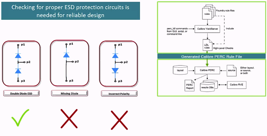
After identifying any potential problems and fixing them, ensuring that all protections are in place, the next step is to verify the geometrical parameters using smart logic-aware physical ESD checks. For example, the ESD diode anode-to-cathode spacing that impacts the transient response of ESD diodes dedicated to ESD-HBM protection must be extracted and compared against a maximum value given in the ESD rules manual, to enable the identification of any unsafe diodes in the chip that do not meet the maximum spacing constraint. Compared to conventional design rule checking (DRC) methodology, this logic-aware approach provides many benefits:
- Instead of running verification on the entire design, only ESD devices of interest captured by the pattern recognition engine are checked against a minimum set of DRC-like constraints, which enables much faster run times
- Markers that are usually inserted manually in layouts to identify ESD regions are no longer needed, which eliminates the risk for human error or omission
- Detected errors are reported with logic information (such as the name and connectivity of the diodes, or the I/O pad name), which is very helpful at analyzing DRC-like reports including geometrical shapes only
One way to implement such a comprehensive ESD flow is by using an automated reliability verification solution to drive all steps of the ESD analysis process from power domain definition to the debugging phase within a comprehensive and reliable ESD analysis framework [1]. With the reliability demands of today’s complex designs, designers must be able to confidently root out and resolve reliability issues to ensure success.
References
[1] J. Lescot, P. Dehan, W. Boujarra, D. Medhat and S. Billy, “A comprehensive ESD verification flow at transistor level for large SoC designs,” 2015 37th Electrical Overstress/Electrostatic Discharge Symposium (EOS/ESD), Reno, NV, 2015, pp. 1-6.
doi: 10.1109/EOSESD.2015.7314740
Author
Dina Medhat is a technical lead for Calibre Design Solutions at Mentor Graphics. She holds a BS and an MS from Ain Shames University in Cairo, Egypt.

Liked this article? Then try this –
Video: How to Check for ESD Protection Using Calibre PERC High Level Checks
This article was originally published on www.edn.com