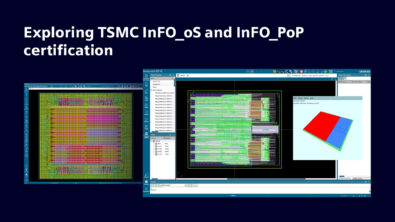
Monolithic scaling limitations drive the growth of 2.5/3D multi-chiplet, heterogeneous integration that enables PPA targets to be met. Our integrated flow addresses prototyping challenges to signoff for FOWLP, 2.5/3D IC, and other emerging integration technologies.

Learn more about semiconductor packaging design and verification.

Featured posts

Latest posts

Image of a chip with text that says: High Bandwidth Memory integration

Managing the complexities of High Bandwidth Memory integration in high-performance computing

The utilization of High Bandwidth Memory (HBM) has become a cornerstone for high performance computing (HPC) CPUs, GPUs, and AI…

Taking 2.5D/3D IC physical verification to the next level

Taking 2.5D/3D IC physical verification to the next level

Taking 2.5D/3D IC physical verification to the next level. As package designs continue to evolve, so must the verification requirements. Designers working on even the most complex multi-die, multi-chiplet stacked configurations require enhanced checking capabilities to quickly and easily verify that the physical die are placed correctly to ensure proper connectivity and electrical behavior.

A deep dive into HDAP LVS/LVL verification

EDA companies are developing tools and workflows to support HDAP (High-density advanced packaging) LVS/LVL verification. Though the data for achieving “signoff-level” confidence is a work in progress, EDA companies are providing tools that can adapt to different levels of data availability and enable HDAP designers to execute HDAP LVS/LVL flows that are both productive and beneficial.

Siemens 3D IC heterogeneous semiconductor packaging workflows catapult design teams into the future of IC design today.

Workflows for tackling heterogeneous integration of chiplets for 2.5D/3D semiconductor packaging

Workflows for tackling heterogeneous integration of chiplets for 2.5D/3D semiconductor packaging.

Image of a chip on a board with text that says Navigating complexities in power delivery analysis: embracing the shift-left approach

Navigating complexities in power delivery analysis: embracing the shift-left approach

The demand for increased power and performance in semiconductor packages has surged. As more die and chiplets are integrated into…

Parasitic extraction technologies: Advanced node and 3D-IC design

Advanced nodes and 3D-IC packages require new and enhanced parasitic extraction processes that can resolve a variety of complex parasitic issues in these designs.

System-level, post-layout electrical analysis for high-density advanced packaging (HDAP)

HDAP designs like FOWLP need post-layout simulation (analog) and post-layout STA (digital) flows to augment basic physical verification DRC and LVS.

Crossing the chasm: Bringing SoC and package verification together

3D IC package designers need assembly-level LVS for HDAP verification.

Package designers need assembly-level LVS for HDAP verification

While advanced integrated circuit (IC) packaging is a fast-growing market, comprehensive package verification still has a ways to go. Unique…