Explore the full Streamlining 3D IC design eBook series and discover how Siemens methodologies and tools can help your team accelerate innovation, improve design quality, and manage the complexity of advanced 2.5D and 3D IC development.
If you are planning to design a high-performance multi-chiplet heterogeneously integrated package, then you know that to achieve design performance, the integration between the logic chiplets is key.
The rules of semiconductor scaling have changed. With traditional transistor scaling slowing, advanced packaging has emerged as the primary driver…
As 3D IC systems continue to scale in complexity, multiphysics is no longer a specialized late-stage activity. It is becoming a core requirement for building designs that can be manufactured successfully and meet long-term performance and lifetime targets.
Siemens partnered with Intel Foundry to develop a STCO centric capability that enables a “smart path” to homogeneous disaggregation using Hierarchical Device Planning and parameterized pin regions.
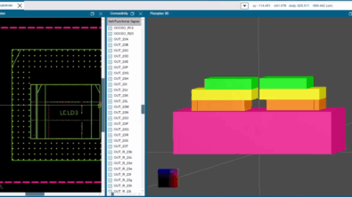
In this blog we will introduce a new way to verify your 2.5/3D IC device assembly level netlist using formal verification that can exhaustively verify all interconnections between the chiplet blocks.
If you have not heard of it before, 3Dblox is an emerging standard that was first created by TSMC but is now managed by IEEE.
Chiplets are revolutionizing the semiconductor industry, enabling unprecedented levels of integration, performance, and flexibility. By breaking complex designs into smaller,…
What is 3D IC technology? 3D IC technology refers to the integration of multiple silicon dies or wafers in a…