Traffic jams & cell libraries: NXP reduces variation risk to boost chip design performance. Learn how!
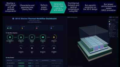
Explore five autonomous EDA workflows demonstrated at NVIDIA GTC Berlin, from spec-to-RTL and design-for-test to physical implementation, design closure and advanced 3D IC design.
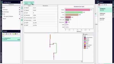
Eliminate post-layout bottlenecks. Solido Layout Analyzer uses AI to connect parasitics and layout-dependent effects directly to circuit performance.
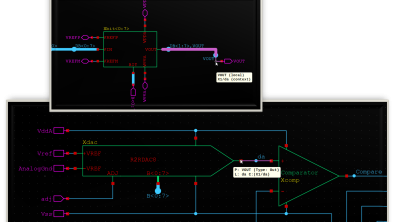
Stop tracing nets by hand. Discover how S-Edit and L-Edit reveal full net connectivity across schematics and layouts without waiting on extraction.
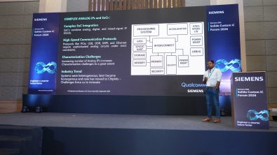
Highlights from Solido Custom IC Forum 2026: AI-powered innovations, agentic EDA workflows and frontline custom chip design and verification
Siemens expands Saskatoon EDA hub, adding 100 jobs and 45,000 sq ft
Siemens EDA’s Mixed-Signal Visualizer simplifies AMS verification by tackling the debug bottleneck with intuitive, holistic views.
At DAC 2026, we announced self-verifying, long-running EDA AI agents for semiconductor and PCB design, in collaboration with NVIDIA.
Join the Solido team at DAC 2026 and explore the latest in agentic AI-powered custom IC design and verification, featuring interactive demos and expert sessions not to be missed.