Accelerate IP design cycles and reduce costs with Calibre design stage verification
By Terry Meeks
In the fast-paced world of semiconductor design, time is a critical asset. One way IC designers save time is to incorporate intellectual property (IP) in their designs, so they don’t have to develop all the chip functionality for every new IC layout. As a result, IP designers and verification engineers face constant pressure to deliver high-quality IP blocks quickly while keeping costs in check. Siemens EDA’s Calibre® platform offers a transformative approach with its design stage verification, allowing teams to shift verification earlier in the IP design flow. This strategic shift left approach maximizes return on investment (ROI) by reducing costs and expediting the IP design cycle while preserving confidence in the quality of the IP.
The challenges of traditional verification
Traditional verification methods call for physical, circuit and electrical signoff verification after the design’s physical implementation is complete. For IP (either hard, soft or custom) confidence in the signoff results is of paramount importance. IP providers do not want their customers finding issues in the IP when it’s verified in the full-chip context later. For IP designers, the growing complexity of IP blocks can extend the verification timeline and increase the chances of errors. This puts immense pressure on design teams to deliver quality IP within tight timelines. Within todays demands for IP time-to-market and quality, the traditional flow increases the risk of costly rework and project delays.
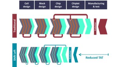
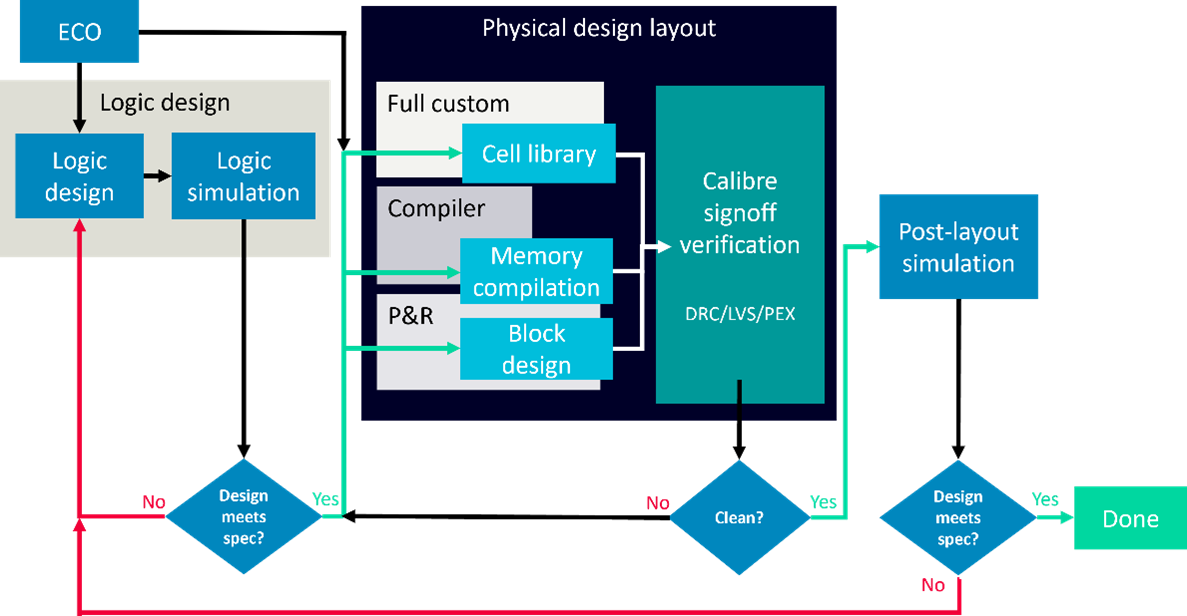
Figure 1 shows a traditional IP design flow through Calibre signoff physical verification (PV). On the left side of the image, the designers create the logic and perform simulation to make sure it will meet the functional and performance requirements. The design (for hard IP) is then physically implemented either as full custom (for cell libraries), with memory compilers or through place and route tools. The physical implementation is checked against foundry design rules in a process that requires write-out and read-in of GDSII or OASIS file formats between the different tool environments. Any errors found then trigger a series of iterations that continue until the design is error-free. Finally, the design goes through parasitic extraction and post-layout simulation. If changes are required to the design, they can be introduced as engineering change orders (ECOs) that require more iterations.

This design and verification flow has worked well for decades, but for large and complex designs that strain engineering and compute resources and that also have faster time-to-market requirements, we need to adjust the flow to achieve greater efficiency, manage costs and reduce time-to-market while ensuring design quality and performance.
Calibre shift left strategy for design-stage verification
Calibre design stage verification offers a shift left strategy that addresses these challenges head-on. By moving verification to earlier stages of the design process, IP designers can identify and resolve issues sooner, resulting in significant cost and time savings. Key benefits of Calibre design stage verification include:
- Early defect detection: Identifying potential issues early on can prevent costly rework later in the design cycle.
- Reduced verification cycles: By integrating verification into the design process, engineers can catch issues as they arise, reducing the number of verification cycles needed.
- Improved efficiency: Calibre’s automated verification capabilities streamline workflows and improve overall efficiency.
The heart of a shift left strategy takes advantage of the fact that the IC design flow is not—as commonly presented in flow charts—a linear process of discrete steps, where one stage completes before going to the next. The reality is that many aspects of the design are in play simultaneously. Much of the process can be compared to a symphony warming up. IP is just one instrument in the symphony. The design or integration happens in parallel with multiple design processes to produce the final system-on-chip (SoC).
Discover more about how Calibre can streamline your design process here.
Maximizing ROI with Calibre
IC companies that buy external IP rely on the quality and performance of those IP, so failure to meet expectations directly impacts the market success of commercial IP companies. For the IP designers, using a single foundry-trusted verification tool suite ensures design rules are checked and errors corrected consistently and with signoff-level quality at every stage of the IP design flow.
The Calibre platform is used by all major foundries to develop new technology node processes. Over 90% of semiconductor design companies use Calibre for their signoff physical verification and design optimization. With the Calibre design-stage verification, IP designers have access to the same advanced verification and optimization functions, plus the underlying rule decks and engines, used by the Calibre platform for signoff verification. When IP design teams perform early design stage verification with Calibre, they can have confidence that design issues will be accurately identified and corrected with signoff-quality fixes (figure 2).

Integrating Calibre design stage verification into your IP design flow can have a profound impact on your bottom line. Here’s how it helps maximize ROI:
- Faster time-to-market: By reducing verification cycles and catching issues early, Calibre speeds up the overall design cycle, allowing you to deliver IP blocks more quickly.
- Lower costs: Early detection and resolution of issues save both time and money, minimizing the need for costly fixes later in the process.
- Enhanced IP quality: By verifying designs early and often, Calibre ensures higher-quality IP blocks with fewer defects, enhancing your reputation with clients.
For more details about the Calibre shift-left verification strategy for IP designers, download our technical paper, A Game Changer for IP Designers: Design Stage Verification.
Customer case study
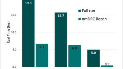
For a company like Marvell, addressing chip assembly and physical verification is a multi-dimensional challenge. Integrating designs with many IP, incomplete blocks and huge file sizes can lead to impossibly long verification times that can derail the tape out schedule. Additionally, the demands of advanced process node design rules leads to a substantial number of violations throughout IP and chip physical verification stages. Learn how the Marvell CAD team enhanced their flow to include Calibre DRC Recon, Calibre LVS Recon, Calibre PERC and Calibre DRC split jobs.
Watch the video of Qi Wang and Paul Dorweiler of Marvell presenting Accelerating design and tapeout: getting large die designs to PV closure.
Get started with Calibre design stage verification
Ready to cut costs and speed up time-to-market in your IP design projects? Calibre shift-left design stage verification is the key to achieving cost and time savings while maintaining high-quality standards. By shifting verification left, you can unlock new levels of efficiency and productivity in your IP design flow.
Learn more about Calibre design stage verification and how it can benefit your projects by visiting the Calibre design stage verification page.