Using a shift left strategy to address block/chip design challenges during design-stage verification
By David Abercrombie
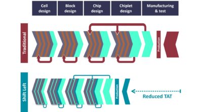
For IC designers, striking the right balance between tight deadlines and limited resources is a constant challenge. Designers are constantly working to enhance efficiency without compromising on design quality. Traditionally, IC design and verification followed a linear process, but modern IC designs require a more concurrent approach that addresses block/chip layout and circuit issues earlier in the design flow. A new approach that provides signoff-quality verification in early design and implementation stages is empowering designers to tackle verification challenges earlier. This “shift left” in design verification can boost productivity, speed up time to market, and improve overall design quality.
Challenges in block/chip design verification
Navigating concurrent design processes
Block and full-chip designers must navigate the complexities of concurrent design processes, which often means designing in-house intellectual property (IP) cells simultaneously with macro blocks and top-level system-on-chip (SoC) designs. However, this simultaneous approach results in overlapping iterations, creating a web of verification challenges. For instance, changes made to lower-level IP cells can impact pin locations, affecting routing in top-level designs. Key decisions about power distribution and clock trees must be made before lower-level components are completed, leading to multiple time-consuming iterations at every design level.
Managing multiple activities and tools
Each block/chip integration iteration involves a series of activities and internal iterations. Traditionally, design creation happens in place-and-route (P&R) tools, while physical verification, static timing analysis, and reliability verification occur elsewhere. This workflow involves constant data transfers, external review/debug cycles, and re-entry into P&R tools. This process can be time-consuming, especially during initial routing and chip finishing when IP designs are at their earliest stages.
Managing time and resources
Early design rule checking runs can require long runtimes and result in millions of errors. Analyzing the error results to determine which errors are relevant at this stage, and then debugging and fixing those errors, can take design teams many hours, if not many days.
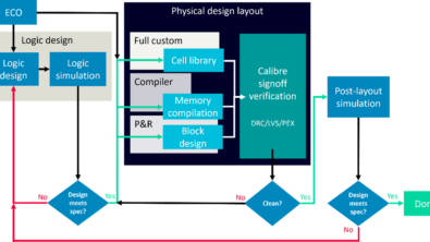
Calibre shift left solutions: A game-changer
Recognizing the need for more efficient design-stage verification, Calibre Design Solutions introduced innovative solutions that shift crucial design verification activities to earlier stages. The tools and techniques comprising these solutions enable block/chip designers to significantly increase productivity, speed up time to market, and elevate design quality.
Benefits to designers
- Signoff-quality verification in design implementation
- The Calibre nmDRC Recon tool analyzes the DRC checks and automatically identifies check categories that can be disabled during initial runs. This selective DRC results in a substantial reduction in runtimes, with an average improvement of 60% to 80%.
- Using the Calibre Auto-Waivers tool in combination with Calibre nmDRC Recon targeted verification further fine-tunes and manages layout verification by suppressing irrelevant DRC errors within IP blocks, enhancing designer focus and reducing runtimes by approximately 50%.
- Early design stage LVS verification
- The Calibre nmLVS Recon tool offers specialized use models that streamline short isolation analysis and short paths debugging, as well as targeted electrical rule checking and compare functions. This concentration reduces iteration cycles and speeds up error debugging by enabling block/chip designers to select and focus on specific areas of interest and the most impactful nets.
- Early design stage error debug
- The Calibre RealTime Digital interface integrates qualified Calibre verification into the P&R tool, allowing designers to make changes locally and assess their impact immediately, without data streamouts. Not only does this integration reduce lengthy debug iteration cycles, but applied fixes remain Calibre-clean throughout the design flow, further reducing signoff iterations.
- Early design stage design optimization
- Calibre shift left solutions go beyond verification to provide selective layout optimization. The Calibre DesignEnhancer tool provides three use models for automated Calibre-clean insertion of vias, metal, decoupling capacitor (DCAP) and filler cells, resulting in significant improvements in electromigration (EM) resistance and voltage (IR) drop.
- Multi-physics verification solutions
- The mPower tools provide block/chip designers with full-chip EM and IR drop analysis. The mPower Digital tool offers fast, precise, and scalable power integrity analysis, even for complex system-on-chip (SOC) designs. Its non-proprietary formats seamlessly integrate into all design and verification flows, making it user-friendly and efficient.
- Workflow optimization
- Siemens EDA continually optimizes the execution environment to simplify and standardize job execution and management. The user-friendly Calibre Interactive interface facilitates scheduling, optimization, and management of multiple Calibre jobs. The reusable hierarchical database (RHDB) eliminates redundancy in HDB construction, saving significant runtime during split runs and enhancing workflow efficiency.
Conclusion
Concurrent design processes have become the norm in IC design, posing challenges for designers. Designers who must shift between different tools and rule decks to verify layouts in different design stages must be diligent to ensure that they, their customers, and the foundries do not experience unexpected results during signoff and tapeout due to inconsistencies. For block/chip designers, Calibre shift left solutions provide a single foundry-trusted source for design verification and optimization, as well as increased efficiency, reduced runtimes, simplified debugging, and innovative design optimization. The key to success lies in employing industry-leading tools like the Calibre nmPlatform throughout the design verification flow. Embracing these solutions unlocks the full potential of IC design in the modern age.
Learn more in our technical paper Navigating design challenges: block/chip design-stage verification