Mastering parasitic extraction at the 3 nm process node
By Dilan Heredia and Karen Chow
Designing integrated circuits (ICs) for the 3 nm process node poses challenges never seen before. One of the biggest challenges for the 3 nm node is the introduction of GAAFETs, including how to model their parasitic capacitance and resistance, given their impact on circuit performance and the significant effect they have on power consumption. Fast, accurate parasitic extraction (PEX) is essential to design success at any node; overcoming design challenges to achieve this goal requires electronic design automation (EDA) PEX tools with advanced extraction capabilities.
What is the 3 nm technology node?
Compared to the 5 nm technology node, the 3nm technology node has the potential to deliver even more improvements in performance, power consumption, and size. This technology introduced gate-all-around (GAA) transistor architecture in place of the finFET transistor architecture used in 5 nm designs. The GAA architecture removes substrate doping and reduces stacking height and source-drain resistance, enabling faster performance with reduced power consumption and smaller size.
Why do we need finFETs and GAAFETs?
FinFET and GAAFET technologies were introduced at advanced nodes to combat unwanted FET physical effects that came with shrinking transistor sizes. Earlier MOSFETs with planar gates didn’t suffer from these effects because they had long channels. As FET gate lengths scaled toward 25 nm, short-channel effects (SCEs) became more and more pronounced, significantly weakening gate control over the channel. With weak channel control, leakage currents become a critical problem that can only be overcome by gaining back the once-strong channel control through new transistor designs.
FinFETs have a double or triple gate structure wrapping around a vertical channel that looks like a fin. FinFETs offer strong channel control at small channel lengths, but they still suffer from SCEs at extreme scaled process features, like gate length or tall fin profiles.
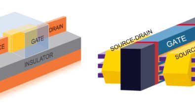
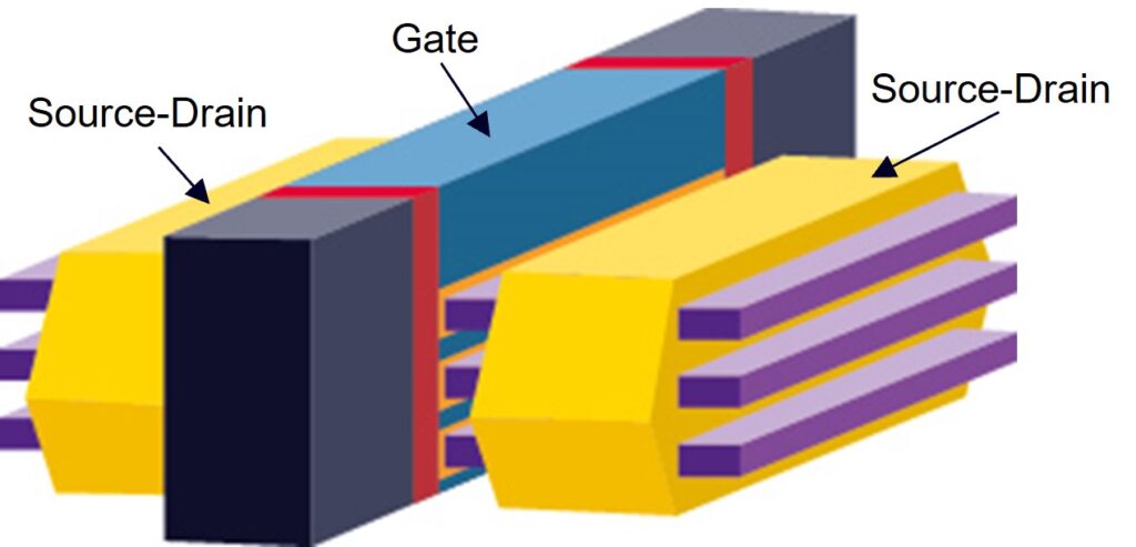
In contrast to finFETs, GAAFET gates fully wrap around the channels (figure 1), allowing for superior control over SCEs. Nanosheet GAAFETs also contain vertically stacked horizontal channels that allow for larger effective channel widths than finFETs without a 2D footprint increase. Designers can use this vertical real estate where needed instead of using x-y space when sizing wider finFET devices.
Parasitics and advanced FET devices
Parasitic capacitance
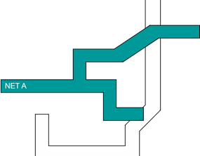
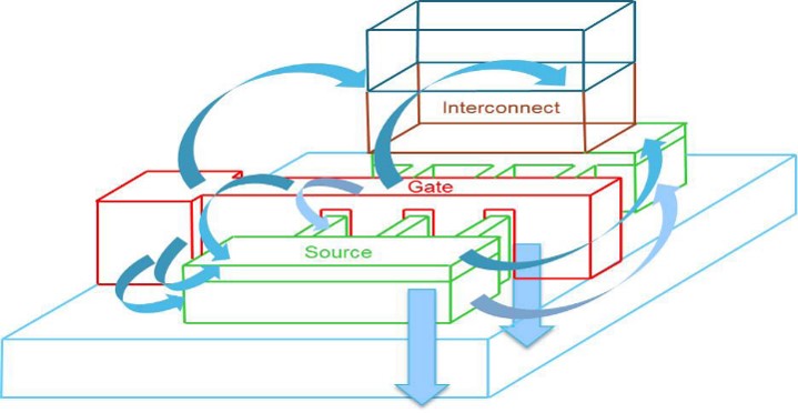
Complex parasitic capacitance interactions at the finFET and GAAFET device level require the highest level of extraction accuracy. These devices have an infinite number of possible FET cell configurations with slightly varying source-drain and gate-via locations. Vias can be placed on the source-drain, active gates, or on the gate material outside the active FET area. Slight geometry and distance variations can affect multiple coupling capacitances within the device, which in turn affect device performance. Traditional rule-based extraction tools using pattern matching around the devices cannot effectively capture all the possible variations and their corresponding effects in a 3D FET device with complex device, interconnect, and dielectric geometries in close proximity to each other (figure 2).
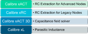
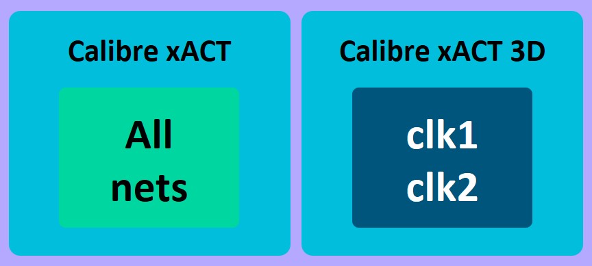
To accurately extract parasitic capacitance interactions around these transistors, a field solver is required . Field solvers are geometry-agnostic, enabling them to perform accurate PEX around finFET and GAAFET devices regardless of the layout. However, because field solvers directly solve the electric fields from the geometries instead of using rule-based equations, they can require longer runtimes. To enable design teams to manage PEX runtimes, the Calibre® xACT™ tool contains a hybrid-engine parasitic resistance and capacitance extractor that uses its fast, rule-based engine for back-end-of-line (BEOL) layers, and its deterministic, mesh-based 3D field-solver to calculate the parasitic capacitances in the front-end-of-line (FEOL) and middle-of-line (MOL). Designers may also use the field solver on certain critical routing nets using the “xACT 3D Select” extraction mode (figure 3).
Multi-corner extraction
Geometries drawn in layouts differ from the actual geometries patterned during fabrication due to systematic, multi-patterning, and random process variations. Modeling these variations is required in advanced extraction flows because interconnect and dielectric geometry variations can significantly influence parasitic capacitances and resistances. For example, if two metal lines turn out to be narrower than expected, they will suffer from greater than expected parasitic resistances. In the case of double patterning mask shifts, the metal lines will be placed closer or further apart, making their coupling capacitance different. These variations can result in a significant performance difference in advanced nodes. Advanced PEX tools must account for these deviations, as well as other factors like temperature variations.
To account for the issues of process and temperature variations, designers use a statistical approach that includes nominal, best, and worst corner scenarios. For example, the worst corner scenario in a specific node or design type can include the worst and least likely coupling capacitance corners, in which double patterning masks are significantly misaligned. A PEX run including models of these scenarios yields different results than the nominal scenario. If the design passes all corner cases in post extraction simulation, it will be a good indicator that the design will work as expected.
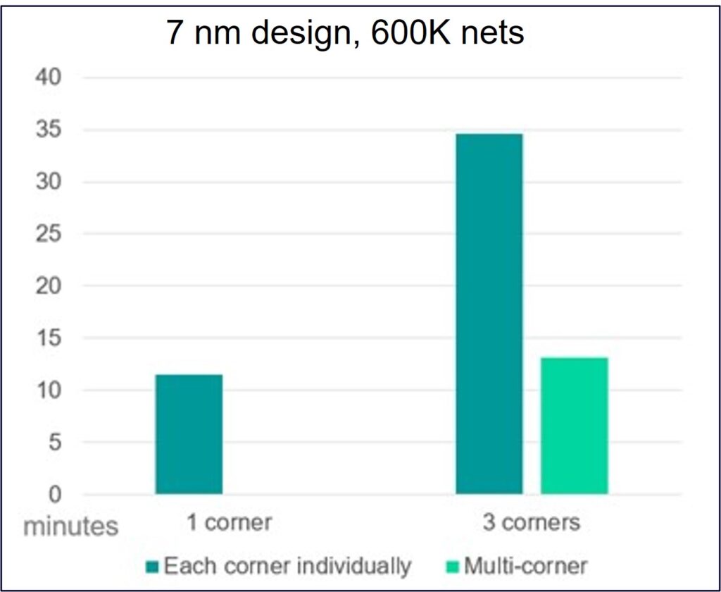
Both the Calibre xACT and Calibre xACT 3D tools offer a multi-corner extraction solution that efficiently addresses process and temperature corner scenarios by extracting best, nominal, and worst corner cases simultaneously in a single run. The necessary process corners are included in foundry-qualified Calibre decks. This accelerated multi-corner extraction approach allows design teams to verify their design with parasitics still satisfies performance requirements in all included corner scenarios.
Figure 4 highlights the performance advantages of using Calibre xACT multi-corner extraction versus single corner extraction – there is less than a 10% runtime increase per corner compared to the 100% runtime increase per corner using sequential single-corner runs.
Modeling metal fill parasitics
Accounting for metal fill parasitic effects on signal nets is important, but often challenging for designs in progress. Designers may want to perform extraction on a portion of the design to verify a design block will work as expected, but the outside region of the design block is empty because fill hasn’t yet been placed. With the Calibre PEX tools, they can enable a metal fill density modeling option for the extraction run. Extracting the design block with this setting enabled ensures the parasitic output values include the modeled fill effects.
Reducing output netlist size
Output netlist sizes can get large, especially in the newest process nodes. Automated parasitic reduction techniques embedded into the extraction process avoid the risk of ending up with netlists so large they cannot be simulated. The Calibre xACT and Calibre xACT 3D PEX tools provide several different types of reduction strategies for different design types and constraints, such as the time constant equilibration reduction (TICER) and coupled capacitance threshold reduction strategies. Designers can include or exclude parasitic reduction techniques to control the netlist size as desired while keeping the parasitic effects that matter.
EMIR analysis
Electromigration and IR (voltage) drop issues are especially significant in advanced technology nodes. With the Calibre xACT tool, designers can easily add the appropriate netlist options to include parameters for subsequent use in EMIR tools. The Calibre xACT output will contain all the needed parameters for the EMIR flow.
If you’d like more details about the capabilities of the Calibre advanced parasitic extraction functionality, including modeling other 3 nm effects like oxide definition spacing or metal boundary impacts, read the full technical paper: Efficient and accurate parasitic extraction for leading-edge process node IC designs