3D IC design solutions: 2024 – Year in review

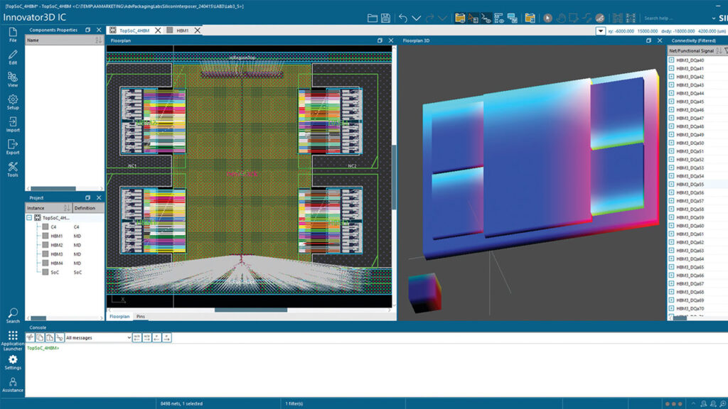
Welcome to a look back at a landmark year in 3D IC technology — 2024 was nothing short of revolutionary! Siemens EDA has been at the forefront of 3D IC, steering the course from the pivotal moments at the Chiplet Summit to the insightful sessions at the Siemens 2024 User2User conference. A crown jewel of the year was undoubtedly the announcement of Innovator3D IC, our new multiphysics cockpit designed for unparalleled 3D IC design verification and manufacturing. As we reflect on a year where Siemens EDA has continued to sculpt the technological landscape of tomorrow for 3D IC, dive into this post to discover how we’re not just following the future but creating it.
2024 Highlights: Siemens EDA redefined the future of 3D IC technology
Revolutionary announcement:
Siemens already had the most comprehensive portfolio of semiconductor packaging related technologies available as part of Siemens Xcelerator, by combining these with Innovator3D IC we enable customers to achieve the realization of more-than-Moore.”
AJ Incorvaia, Sr. VP of Electronic Board Systems at Siemens Digital Industries Software
Significant events & milestones:
- Chiplet Summit: Access the 2024 proceedings
- TSMC 2024 NA OIP Ecosystem Forum: Access the full list of Siemens EDA papers
User2User 2024 conference insights: Watch the session recordings on demand!
- Pioneering semiconductor reliability automotive apps – imec’s Canary chip
- Customer-specific solutions with Siemens EDA tools: Sysberry GmbH
- Meeting future performance demands through packaging: ChipletZ
- Silicon photonics to integrate chiplets: Swissbit
- Chiplets for future automotive application: Fraunhofer
- EMIB based advanced packaging flow – Intel Foundry
- xPD xSI PDK design enablement – Beyond Xpedition templates – Siemens
- Assembly verification flow for silicon interposers – Broadcom
- Advanced physical verification flows for 3D IC’s – Microsoft
White papers:
- Parasitic extraction technologies: Advanced node and 3D-IC design
- A deep dive into HDAP LVS/LVL verification
- Taking 2.5D/3D IC physical verification to the next level
- New innovative way to functionally verify heterogeneous 2D/3D package connectivity
Infographics:
- Discover how AI is changing the nature of semiconductor design
- The role of AI-infused EDA solutions for semiconductor-enabled products and systems
- The multi-physics challenge: Known good die may not behave in 3D IC as stand alone!
- Why is a comprehensive workflow essential for chiplet design and today’s 3D IC architectures?
- The evolution of machine learning (ML) in the physical design and verification of semiconductor packages
eBook:
Videos:
- Workflows for tackling heterogeneous integration of chiplets for 2.5D/3D semiconductor packaging
- Taking 3DIC heterogeneous integration mainstream
- EE Times Fireside chat: Linking design to manufacturing for a sustainable semiconductor future
The way the industry’s going – when we look at the tools and the methodologies that we need – it’s starting to move from just talking about semiconductors to talking about entire systems.“
Michael Munsey, VP at Siemens EDA
Dive deeper and discover more!
Don’t miss out on the cutting-edge insights that are shaping the future of 3D IC technology. Explore, learn, and leverage these groundbreaking resources now to stay ahead in the semiconductor industry.
As we set our sights on 2025, we’re dedicated to continuing our tradition of innovation and excellence. Prepare to pioneer the next wave of technological advancements with Siemens EDA and stay at the forefront of the 3D IC semiconductor industry.
To learn more about Siemens EDA 3D IC solutions, visit the 3D IC Homepage
- Read a case study: Smarter, faster, greener AI with 3D IC chiplet advanced packaging
- Explore a curated selection of 3D IC assets
- Access the 3D IC Resource Library
- Visit the 3D IC blog site to learn more about the latest in 3D IC
- Listen to the 3D IC Podcast
Contact us to learn more about our 3D IC design solutions


