Taking 2.5D/3D IC physical verification to the next level
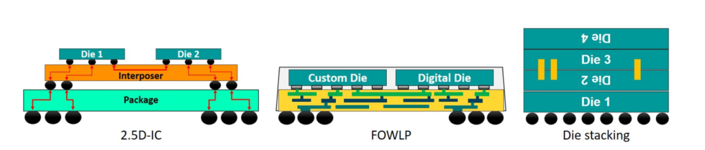
The adoption of high-density advanced packaging (HDAP) continues to grow for all kinds of end-user applications. 2.5D integrated circuit (IC) designs using interposers (silicon or organic) generally target high-end applications such as military, aerospace, and high-demand computing, while 3D fan-out packaging approaches like the TSMC integrated fan-out (InFO) package focus more on mass consumption consumer applications like cell phones. As a result, major design houses, foundries, and outsourced semiconductor assembly and test (OSAT) companies are investing in the next level—true die stacking using through-silicon vias (TSVs) and hybrid bonding. Verification for these HDAP devices is complex and requires a new design-to-manufacture paradigm.
HDAP technologies
How do EDA tools approach HDAP verification?
Electronic design automation (EDA) support for HDAP verification has evolved right along with the use of HDAP designs. Multiple issues related to HDAP verification have been addressed in HDAP verification solutions.
For example:
- The development of assembly design kits (ADKs) for package designs.
- Concept of and requirements for assembly-level LVS for advanced packaging.
- Post-layout analog simulation and digital static timing analysis (STA) flows for advanced packaging.
- Options for generating HDAP system-level connectivity while accounting for die, package, and die/package interface parasitics.
- Verification options to address “data incompleteness” in 3D IC verification.
What are the requirements for HDAP verification?
In its simplest form, HDAP physical verification consists of two major requirements:
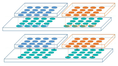
- Connectivity: verifying that multiple die are connected correctly though the package/interposer routing
- Alignment: verifying that multiple die are aligned as expected on top of the package/interposer
This basic definition of 2.5/3D IC physical verification is generally considered to be well-established – meaning both the end customers and the ecosystem partners are aware of and understand the essential requirements. In fact, ecosystem collaboration was the driving force behind the development of 3D IC physical verification design kits that were the beginnings of package ADKs.
How can EDA tool verification keep pace with HDAP advancements?
As 3D IC technologies advance and design companies build more complicated HDAP designs, physical verification requirements are expanding. These advanced physical verification requirements are taking 3D IC physical verification to the next level. To keep pace, EDA suppliers are expanding the capabilities of their 3D IC verification tools and strategies.
For example:
- Designers will need to perform signoff design rule checking (DRC) and LVS verification.
- Critical alignment checks must be enhanced.
- Die/interposer alignment checking is an essential step performed during 3D IC verification.
- False errors in interposer-to-die checking.
- Debugging centers check misalignment errors.
- Centers check for texted bumps/pads.
How do you manage missing or incomplete 3D IC data?
One of the challenges that many design teams face in 3D IC verification flows is effectively managing incomplete data and incorrect setups.
- Missing data in the input
- Missing alignment checks
- Systemic issues like differences in pin names between layout and source, etc.
To minimize these impacts, an innovative precheck mode that allows designers to capture any obvious setup/data issues must be provided. This precheck mode helps catch any early systemic system-level/multi-die integration issues before the signoff run. The precheck mode must include multiple processes for data and setup issue detection including:
- Source netlist checking
- Checking for texted pads
- Missing or extra port checking
- Deck coverage
- Power and ground short checking for interposer, etc.
Rising to the challenges of 2.5D/3D IC physical verification
To recap, as package designs continue to evolve, so must the verification requirements. Designers working on even the most complex multi-die, multi-chiplet stacked configurations require enhanced checking capabilities to quickly and easily verify that the physical die are placed correctly to ensure proper connectivity and electrical behavior. This includes a precheck mode that enables design teams to find and correct basic implementation mistakes and systemic errors before invoking the signoff run – thus eliminating unnecessary debugging iterations and speeding up the overall package verification flow.
Solutions for 2.5D/3D IC physical verification
Discover how Siemens’ heterogenous 3D IC solutions including Calibre 3DSTACK perform the physical verification and prechecks that enable design teams to find and correct basic implementation mistakes and systemic errors before signoff. Additionally, integration with Siemens Xpedition Package Designer (XPD) and Xpedition Substrate Integrator (XSI) helps speed implementation, empowers design companies to enhance the market value of their products further and provides a more fully automated design-to-manufacture paradigm for the HDAP industry.
To learn more about taking 2.5D/3D IC physical verification to the next level read this white paper written by John Ferguson, Product Management Director, and Armen Asatryan, R&D Technical Lead for Advanced Packaging Solution at Siemens EDA.
Want to learn more about 3D IC technology?
- Listen to The future of semiconductor design podcast, in which industry experts discuss 3D IC concepts and the latest trends: chiplet designs, IC packaging, multi-die verification, golden netlists, electrical signoff, system analysis, and more!
- Read The beginner’s guide to 3D IC to discover how 3D IC is evolving.
- View this infographic to learn how toUnlock the potential of 3D IC.
- Learn more about 3D IC front-end design planning and predictive analysis in this ebook entitled “Launching the full potential of 3D IC with front-end architectural planning”
- Discover the 3D IC design workflows available to designers in this eBook entitled: Semiconductor packaging: making the right connections in 3D IC design


