Taking 2.5D/3D IC physical verification to the next level

Taking 2.5D/3D IC physical verification to the next level

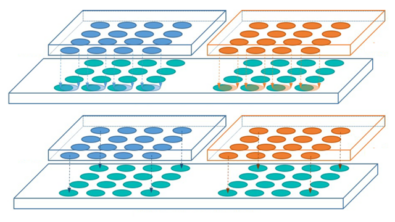
Taking 2.5D/3D IC physical verification to the next level. As package designs continue to evolve, so must the verification requirements. Designers working on even the most complex multi-die, multi-chiplet stacked configurations require enhanced checking capabilities to quickly and easily verify that the physical die are placed correctly to ensure proper connectivity and electrical behavior.

A deep dive into HDAP LVS/LVL verification

EDA companies are developing tools and workflows to support HDAP (High-density advanced packaging) LVS/LVL verification. Though the data for achieving “signoff-level” confidence is a work in progress, EDA companies are providing tools that can adapt to different levels of data availability and enable HDAP designers to execute HDAP LVS/LVL flows that are both productive and beneficial.

Parasitic extraction technologies: Advanced node and 3D-IC design

Advanced nodes and 3D-IC packages require new and enhanced parasitic extraction processes that can resolve a variety of complex parasitic issues in these designs.

System-level, post-layout electrical analysis for high-density advanced packaging (HDAP)

HDAP designs like FOWLP need post-layout simulation (analog) and post-layout STA (digital) flows to augment basic physical verification DRC and LVS.

Crossing the chasm: Bringing SoC and package verification together

3D IC package designers need assembly-level LVS for HDAP verification.

Package designers need assembly-level LVS for HDAP verification

While advanced integrated circuit (IC) packaging is a fast-growing market, comprehensive package verification still has a ways to go. Unique…

Image of a boulder in a desert

A “big rock” approach to DC drop analysis in IC package design

The key analysis needs of high-performance computing semiconductor package design Today, power requirements are continually increasing as you bring more…

Illustration of an IC Package design with text that says Why are you spending 30%+ more time on semiconductor packaging design?

Why are you spending 30%+ more time on semiconductor packaging design?

Designs are just getting bigger and more complex Yes, an obvious aspect is increasing design complexity. Packages are now a…

Image of a semiconductor package design

What are the top challenges of high-performance computing/AI semiconductor package design?

If you’re designing a high-performance processor-based package,  it’s common for the semiconductor package design to contain multiple logic chips that…