Crossing the chasm: Bringing SoC and package verification together

Accurate verification of fan-out wafer-level packaging (FOWLP) designs requires the integration of package design environments with system-on-chip (SoC) verification tools to ensure package manufacturability and performance.
Wafer-level packaging (WLP) certainly enables higher form factor and improved performance compared to traditional SoC designs – however, to achieve acceptable yield and performance – electronic design automation (EDA) companies, outsourced assembly and test (OSAT) companies, and foundries must collaborate to establish consistent, unified, and automated die-level signoff verification to 2.5D and 3D stacked die assemblies. This includes fan-out wafer-level packaging (FOWLP), to ensure manufacturability and performance – while introducing minimum disruption to existing package design flows.
Wafer-level packaging
WLP is a promising “More than Moore” technology that enables higher form factor and improved performance compared to traditional SoC designs. Unlike 2.5D and 3D integrated circuit (IC) designs, WLP doesn’t require through-silicon vias (TSVs), which are expensive and may cause mechanical and thermal reliability issues.
There are two WLP styles predominantly in use: fan-in and fan-out. Both of these styles enable single-die and multi-die integration. However, for the multi-die fan-in process, multiple dies are typically from the same silicon wafer (homogenous integration). In the case of FOWLP, the die integration can be either homogenous or heterogeneous. FOWLP design for example utilizes the package-level redistribution layers (RDLs) to connect from the die to external ball grid arrays (BGAs), and between die in multi-die configurations.
FOWLP design and verification
From an IC packaging perspective, package design and verification flows are much simpler than those used for SoCs. However, for packaging technologies such as FOWLP the package design and verification process has become much more complicated. Because FOWLP manufacturing occurs at the “wafer level,” it incorporates mask generation, similar to the SoC manufacturing flow. That means solid package design and verification flows must be in place so the designer can ensure the manufacturability of the FOWLP by the foundry or OSAT company. Similar to the PDKs used for an SoC, the foundry or OSAT must now provide the package designer with some form of an assembly design kit (ADK), as shown in Figure 1.
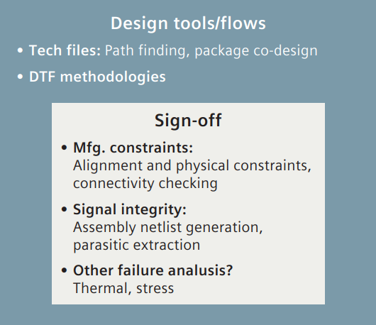
Figure 1 Package ADK components
Addressing the challenges that uniting ICs and packages presents requires new EDA functionality that bridges the gap between the IC world and the packaging world while introducing minimal disruption to the already-existing package design flows. This new design platform must also contain several verification tools that can be used for FOWLP designs that:
- Verify the physical implementation of each die by itself
- Verifies package routing DRC
- Verifies interfaces along with package connectivity and whole system connectivity
This whitepaper written by Tarek Ramadan, 3D IC Technical Team Leader, Siemens EDA entitled “Crossing the chasm: bringing SoC and package verification together with Calibre 3DSTACK” describes why IC package designers need assembly-level LVS for HDAP verification as well as provides insights and solutions that support die-level signoff verification for a wide variety of 2.5D and 3D stacked die assemblies that can ensure manufacturability and performance.
CLICK HERE to learn how you can deliver product differentiation faster using 3D heterogeneous integration of node and performance-optimized chiplets with Siemens EDA’s market-leading 3D IC technology solution.


