For years, data-center performance scaled by following a familiar playbook: faster GPUs, higher SerDes rates, and increasingly aggressive board designs….
Some say we are officially in the Post-Moore’s Law world. Moore himself closed his seminal paper by mentioning the “day…
Headlines on how the global AI race leads to the shortages of GPUs are in no short supply. Behind those…
AI is hot — literally. As we bid farewell to a transformative year of 2025, there’s no doubt that the AI chip underwent substantial changes. As AI compute is pushing…
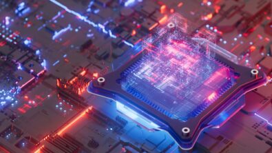
With 3D IC integration blurring the lines between chip and package, is your team’s mindset truly system-centric, or are traditional…
The future of semiconductor innovation is rapidly shifting from monolithic chips to advanced, multi-chiplet architectures. As devices demand greater power,…
Would you risk millions of dollars on a semiconductor design without knowing if it can be manufactured? Discover why test…
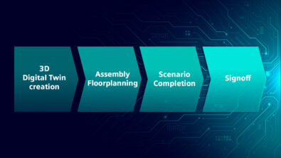
As 3D IC complexity skyrockets, are we truly evolving our design methodologies at the same pace, or are we unknowingly…
Q: Is dedicated SI/PI analysis still necessary in 3D IC design? A: With the rapid advancements in chip design automation…