For years, data-center performance scaled by following a familiar playbook: faster GPUs, higher SerDes rates, and increasingly aggressive board designs….
Some say we are officially in the Post-Moore’s Law world. Moore himself closed his seminal paper by mentioning the “day…
Headlines on how the global AI race leads to the shortages of GPUs are in no short supply. Behind those…
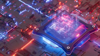
AI is hot — literally. As we bid farewell to a transformative year of 2025, there’s no doubt that the AI chip underwent substantial changes. As AI compute is pushing…
The future of semiconductor innovation is rapidly shifting from monolithic chips to advanced, multi-chiplet architectures. As devices demand greater power,…
Chiplets are revolutionizing the semiconductor industry, enabling unprecedented levels of integration, performance, and flexibility. By breaking complex designs into smaller,…
Integrated circuits (ICs) are the foundation of modern electronics, powering everything from smartphones and medical devices to servers and automotive…
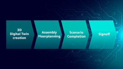
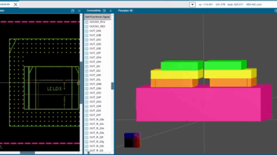
From optimizing connectivity to ensuring electrical performance, designers are tasked with meticulous planning and execution to achieve seamless communication and…
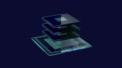
Understanding the evolution and importance of chip packaging As semiconductor innovation pushes the boundaries of performance and power efficiency, chip…