Parasitic extraction technologies: Advanced node and 3D-IC design

Most IC designers adopt advanced process technology nodes to benefit from improved performance, density, and functionality while also reducing delays and power consumption through continuous dimensional scaling. The utilization of new device architectures like fin field-effect transistors (finFET), fully depleted silicon-on-insulator (FDSOI), and gate-all-around GAA transistors extends gate length scaling but also results in increased interactions between neighboring geometries.
While 3D-IC design is growing in popularity by offering device scaling with minimal costs, it requires verifying the parasitic effects between components and interconnects across multiple processes. To ensure accurate capture of parasitic and layout-dependent effects for non-planar devices, new parasitic extraction (PEX) as well as accurate extraction and modeling is necessary for emerging 3D-IC designs. Implementing these PEX solutions into verification flows enables designers to successfully realize the performance and market benefits of their advanced node designs.
Parasitic extraction challenges for 3D-IC:
Advanced nodes: finFETs, non-planar multi-gate structures, and nanowire metal-oxide-semiconductor field-effect transistors (MOSFETS) add new complexity to the extraction process. Managing parasitics in 7 and 5nm designs for example requires a comprehensive approach that includes extensive interconnect modeling and extraction, as well as enhanced design analysis.
3D-IC modeling: Parasitic extraction on 3D-IC packages requires additional effort. For example, FOWLP extraction includes interconnect on both the dies and the package, as well as the interaction between them. When placing two dies with tops together to create a single 3D-IC, it is important to capture the effect of the face-to-face via, as well as the interactions between the top layers of the die.
Parasitic extraction solutions for 3D-IC:
IC interconnect modeling can be split into three different sections:
- Front-end-of-line (FEOL): All of the IC fabrication layers that make up a device (transistors, capacitors, resistors, etc.). Industry device models are used with simulation tools to model FEOL layers.
- Middle-of-line (MOL): MOL layers consist of a series of contacts and local interconnect that connect a device to the metal wires. A field solver is required to accurately model circuit performance in MOL layers as it captures 3D effects most precisely.
- Back-end-of-line (BEOL): Metallization layers where individual devices (transistors, capacitors, resistors, etc.) are interconnected with wiring on wafer. This requires modeling and accurately computing coupling capacitance shifts due to mask misalignment.
More accurate modeling of corners at advanced nodes lets designers optimize layouts to meet design goals.
Multi-corner extraction for 3D-IC
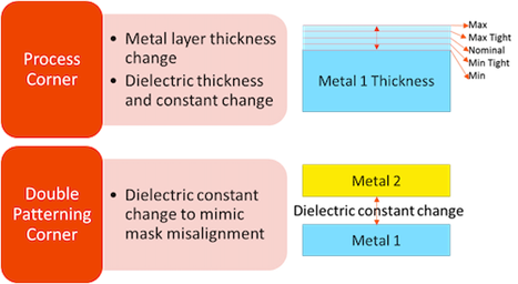
Multi-corner interconnect extraction is a requirement for both custom and digital designers. Not only voltage and temperature, but also cell characterization, block extraction, and signoff must be done at multiple process corners. Multi-patterning at advanced nodes adds even more corners. As designs are also growing in complexity at each successive node, a big challenge is processing the design and the necessary corners without incurring additional cycle time during the signoff phase.
In the past, each process corner meant a separate extraction run. For nine process corners for example, the designer had to run PEX nine times, which required either adding machine resources or extending the PEX time budget.
To solve this challenge at advanced nodes, tools must perform simultaneous multi-corner extraction, in which all process, multi-patterning, and temperature corners are extracted in a single run. 3D-IC modeling is an effective way to improve specifications, but extraction must be applied appropriately. This platform must also enable signoff verification, including parasitic extraction of virtually any 3D-IC configuration, from chip stacks with flip chips, to silicon interposers and through silicon vias (TSVs) ideally without breaking current tool flows or requiring new data formats.
Design analysis for 3D-IC
Due to the increased density and the use of finFETs in these new technologies, self-heating and electromigration (EM) are becoming a big issue. To take self-heating into consideration, tools must provide the device location information to the EM/self-heating analysis, in addition to the standard parameters.
There are several methods to reduce current density – for digital designs, there is via doubling and wire spreading. For analog, mixed-signal, and radio frequency (RF) designs, the main architecture is decided, and the circuits are captured using schematic capture then simulation is run to determine if the design meets specifications.
To learn more about the parasitic extraction processes that advanced nodes and 3D-IC packages require – download this whitepaper entitled “Parasitic extraction technologies- Advanced node and 3D -IC design” written by Karen Chow and Claudia Relyea, Principal Product Engineers at Siemens EDA.
CLICK HERE to learn how you can deliver product differentiation faster using 3D heterogeneous integration of node and performance-optimized chiplets with Siemens EDA’s market-leading 3D IC technology solution.