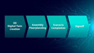
Two such STCO-related activities are now AI-powered in Innovator3D IC Integrator as part of the 2604 release and deliver superior results in an efficient predictable manner.
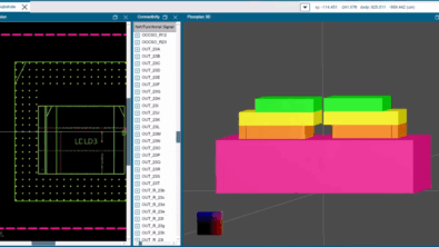
In this blog we will introduce a new way to verify your 2.5/3D IC device assembly level netlist using formal verification that can exhaustively verify all interconnections between the chiplet blocks.
If you have not heard of it before, 3Dblox is an emerging standard that was first created by TSMC but is now managed by IEEE.
With 3D IC integration blurring the lines between chip and package, is your team’s mindset truly system-centric, or are traditional…
The future of semiconductor innovation is rapidly shifting from monolithic chips to advanced, multi-chiplet architectures. As devices demand greater power,…
Would you risk millions of dollars on a semiconductor design without knowing if it can be manufactured? Discover why test…
As 3D IC complexity skyrockets, are we truly evolving our design methodologies at the same pace, or are we unknowingly…
Q: Is dedicated SI/PI analysis still necessary in 3D IC design? A: With the rapid advancements in chip design automation…
Chiplets are revolutionizing the semiconductor industry, enabling unprecedented levels of integration, performance, and flexibility. By breaking complex designs into smaller,…