Workflows for tackling heterogeneous integration of chiplets for 2.5D/3D semiconductor packaging
Keeping pace with Moore’s law continues to be a challenge and is driving the adoption of innovative packaging technologies that support continued system scaling. While doing so at costs less than comparable monolithic devices these packaging technologies disaggregate what would typically be a homogeneous or monolithic device like an ASIC or SoC into discrete unpackaged die known as chiplets. Today these devices are being designed and produced by a small number of advanced users. Broad industry proliferation will require the standardization of chiplet models along with the die-to-die connectivity IP – it will also necessitate workflows that support die package codesign.
What is a chiplet?
The chiplet is a die specifically designed and optimized for operation within a package in conjunction with other chiplets. This is also referred to as heterogeneous integration where multiple die or chiplets are integrated into a system in package (SiP). These devices offer considerable benefits including performance, power, area, cost, and time to market.
Is heterogeneous packaging disruptive?
While heterogeneous integration offers many advantages it can also be disruptive to traditional design methods. Many Siemens customers are finding the need to evolve their methods and tools to fully leverage the benefits of heterogeneous integration.
Examples:
- Transition to system-based optimization from design-based optimization
- Expanding supply chain and tool ecosystems
- Balancing design resources across competing multi-domain requirements
What are the 3 enabling technologies for heterogeneous integration?
The 1st enabler is Die-to-die interface IP. These are the physical files used to implement the high-speed interfaces within the package. UCIe, BoW, and AIB are just a few examples of one of the big benefits of chiplets in close proximity to one. Another is lower power requirements to drive these signals – which is a characteristic of the number of these protocols.
Packaging and assembly technologies is the 2nd enabler. It includes various packaging assembly and substrate technologies. Examples include 2.5D silicon interposers, bridges, or high-density organic substrates.
The 3rd enabler is EDA tools and workflows. These are the integrated design tools, the scripts, etc. needed for chiplet implementation. Most of these tools exist today but what we have are domain-specific tools. We have different tools for packaging for thermal analysis, silicon design, and so on.
What are the primary functions for chiplet-based heterogeneous integration?
Figure 1 below represents the primary functions along with the associated tasks for each step for chiplet-based heterogeneous integration. You’ll notice that Planning and Predictive Analysis is at the center. This is because many downstream issues can be traced back to poor engineering decisions made in the early stages of design. This planning and these predictive modeling functions enable better engineering decisions on resource allocation resulting in higher-performing more cost-effective products.
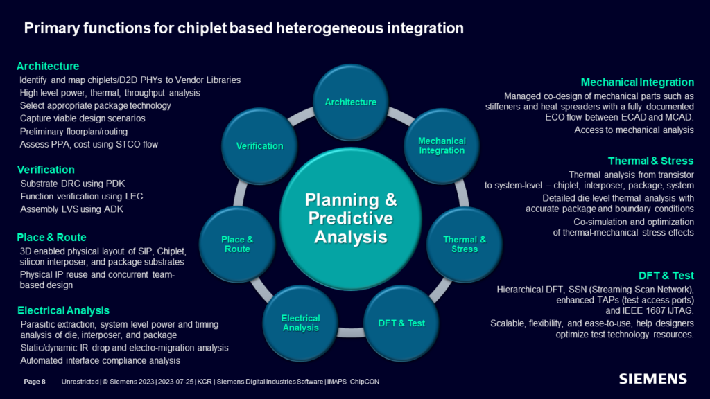
Figure 1
What are the heterogeneous integration workflows?
There are 5 workflows necessary to plan, implement, verify, and continuously qualify that the heterogeneous design meets its performance specification. These 5 workflows span 3 phases of modeling and analysis:
- Predictive Modeling
- In-Design modeling
- Signoff
- The 1st workflow is Architectural planning and analysis. This enables the system and or the RTL designer to rapidly explore and capture viable design architectures leveraging 3 key inputs: the chiplet components in the corresponding design kits, standard high-speed protocols for internal die-to-die interfaces within the package, and then external chip-to-chip interfaces between the sip package and other devices within the system at the PCB level.
- The 2nd workflow is Physical planning implementation and analysis. This workflow applies to both interposers and packaged substrates and includes package floorplanning, file planning, power delivery, substrate route feasibility, and netlist optimization along with all the corresponding checks like LVS and logic equivalency checks.
- The 3rd workflow is Design analysis, this workflow incorporates extraction and simulation tools that support SiP level signal and power integrity, static and dynamic IR drop, electromigration analysis, and static timing analysis. Traditional packaging on-site techniques can be used to simulate the high-speed interfaces, but static timing is needed for the low-speed signals along with the tester control type connections.
- The 4th workflow is Reliability analysis. Two unique areas that require extensive analysis and heterogeneous designs are thermal and mechanical stress. Given the close proximity of devices, there’s a high likelihood of some type of chip-to-chip or chip-to-package interaction occurring. Thermal coupling can be a big concern if not accounted for.
- The 5th workflow is perhaps one of the more challenging workflows for heterogeneous packaging – it is the Test planning and validation workflow for manufacturing tests. It requires a robust DFT infrastructure including enhanced TAP and SSN – It requires wafer-level test, die testing within the package, and interface testing between die. The good news is that we have established TFT standards for testing 2.5D and 3D designs.
Heterogeneous integration key takeaways
There are numerous advantages and benefits of heterogeneous integration that enable larger more complex systems than monolithic alone which also offers improved power performance area and form factor. However, these don’t come for free. There are key challenges that must be met: optimal decomposition and architecture selection, power delivery through the system as well as thermal management, and also timing and tests are all prime examples.
Some of the key takeaways from heterogeneously integrated systems include:
- The need for upfront predictive analysis which is key for architectural and physical planning.
- The need for multi-domain multi-tool design analysis as well as collaboration between the different engineering teams.
- Thermal and mechanical stress also need to be accounted for throughout the design process.
There is no single tool for 2.5D and 3D heterogeneous designs – it’s multiple tools which most, if not all exist today. The effort and the focus needs to be on building, qualifying, and the deployment of the workflows described above.
To learn more about the heterogeneous integration of chiplets for 2.5D/3D semiconductor packaging and the workflows they require watch this informative on-demand webinar presented by Kevin Reinbold, Account Technical Manager for Advanced Packaging Solution at Siemens EDA
Click here to learn how you can deliver product differentiation faster using 3D heterogeneous integration of node and performance-optimized chiplets with Siemens EDA’s market-leading 3D IC technology solution.