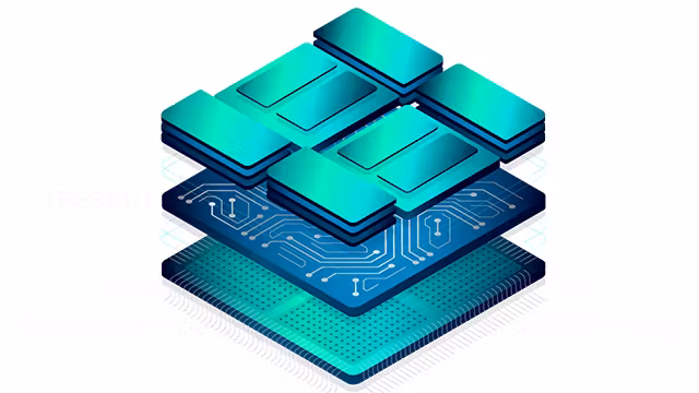
Integrated circuits (ICs) are the foundation of modern electronics, powering everything from smartphones and medical devices to servers and automotive…
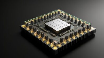
Why 2.5D vs. 3D IC matters in modern chip design As semiconductor innovation pushes the limits of Moore’s Law, traditional…
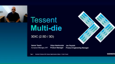
Learn about Siemens’ Tessent Multi-die solution for 3DIC packaging.
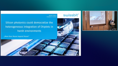
Swissbit is pioneering chiplet and system-on-package solutions that embed security and functional safety from the design phase to meet stringent requirements in harsh industrial and automotive environments.
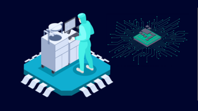
Explore this infographic to learn why a comprehensive workflow essential for chiplet design and today’s 3D IC architectures.
Workflows for tackling heterogeneous integration of chiplets for 2.5D/3D semiconductor packaging.
In our last 3D IC blog, we talked about the impact of 3D IC on device reliability. In today’s blog,…
Semiconductor engineers aim to deliver best-in-class devices despite technology scaling and cost limitations of monolithic integrated circuit (IC) design. To…