2.5D vs. 3D IC: which chip packaging technology is right for you?
Why 2.5D vs. 3D IC matters in modern chip design
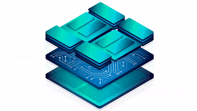
As semiconductor innovation pushes the limits of Moore’s Law, traditional 2D scaling is no longer enough to meet demands for higher performance, lower power, and smaller form factors. That’s where advanced packaging technologies—2.5D and 3D ICs—come in.
Both 2.5D and 3D IC technologies enable heterogeneous integration and greater chip functionality, but their architectures, performance characteristics, and manufacturing complexities differ significantly. Choosing the right approach can impact everything from system cost to thermal management and yield.
In this article, we’ll break down the key differences between 2.5D vs. 3D IC, explore their use cases, and examine how the industry is evolving to support next-generation system designs.
What Is 2.5D IC integration?
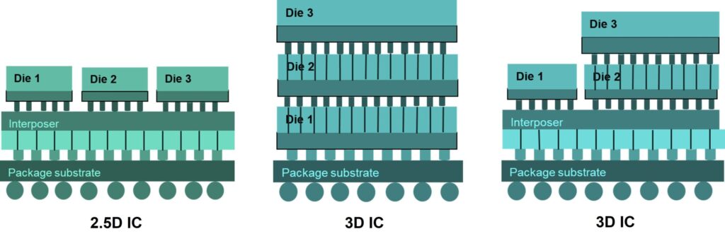
2.5D IC packaging connects multiple bare dies side-by-side on a common interposer. The interposer acts as a high-density substrate that routes signals between dies. Typically made of silicon, organic, or glass, the interposer enables close proximity between chips without stacking them vertically.
Technical Characteristics of 2.5D IC:
- Die placement: Lateral (planar) on interposer, though limited vertical stacking is possible for certain designs
- Interconnects: Micro-bumps, TSVs in interposer (not active dies)
- Materials: Typically uses a silicon interposer for high-performance applications, though glass and organic substrates are also used depending on cost, signal integrity, and thermal requirements
- Thermal profile: Easier to cool due to planar layout
When to Use 2.5D IC:
- High-bandwidth memory (HBM) adjacent to logic
- ASICs, FPGAs, and GPUs requiring scalable IO
- Modular systems with IP reuse across generations
- Shorter development cycles with manageable thermal profiles
Related Resource: Explore Siemens’ IC Packaging Solutions
What Is 3D IC integration?
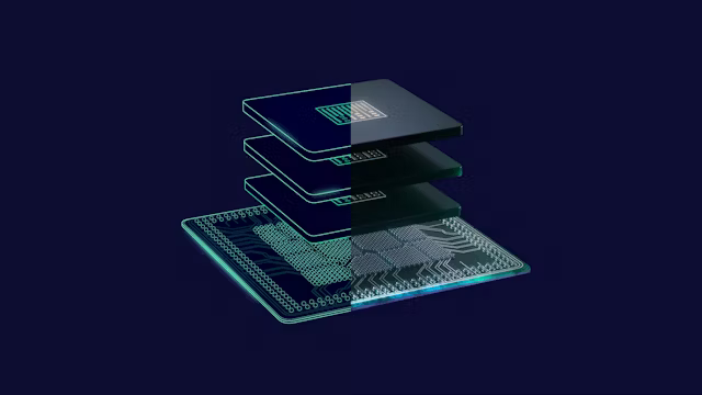
3D IC design stacks multiple active dies vertically, connecting them with through-silicon vias (TSVs) and micro-bumps. This vertical integration enables unprecedented density and performance by shortening interconnect distances and integrating disparate technologies (e.g., logic + memory) in a single package.
Technical Characteristics of 3D IC:
- Die placement: Vertically stacked
- Interconnects: TSVs between active die layers
- Integration: Heterogeneous logic/memory/mixed signal
- Thermal profile: Complex, often requiring advanced cooling solutions
When to Use 3D IC:
- AI accelerators and mobile SoCs with extreme bandwidth needs
- Compact form factors such as wearables and edge computing
- High-performance computing (HPC) with tight area and power budgets
- Advanced heterogeneous integration of compute, analog, and memory
💡 Learn more in our blog: 3D IC Guide to Heterogeneous Integration
How to choose between 2.5D and 3D IC
Key Decision Factors:
| Decision Factor | 2.5D IC | 3D IC |
| Performance Needs | High | Ultra-high |
| Thermal Budget | Easier to manage | Requires advanced thermal management |
| Form Factor Constraints | Moderate | Ideal for ultra-compact systems |
| Power Efficiency | Good | Superior due to shorter interconnects |
| Design Risk | Lower | Higher due to vertical stacking |
| Cost Sensitivity | Lower fabrication cost | Higher (TSV and stacking complexity) |
| IP Reuse | High—same dies used across systems | Moderate—stacking often customized |
🎓 Want a deeper dive into how to select the right packaging strategy?
Read: Chip Packaging—Basics to Advanced 3D IC
Real world applications of 2.5D and 3D IC technologies
Understanding where and how 2.5D IC and 3D IC technologies are applied in real-world systems is essential for choosing the right packaging strategy. Each has distinct advantages, and selecting the best fit depends on performance demands, thermal constraints, form factor, and design complexity.
When 2.5D IC Makes Sense
2.5D integration is well-suited to applications that require high interconnect bandwidth, modular scalability, and simpler thermal management. By placing dies side-by-side on an interposer, 2.5D offers designers a flexible and cost-effective way to boost system performance without the design and manufacturing complexities of stacking.
Common applications include:
- Networking ASICs
- Require scalable throughput and fast design cycles
- Benefit from the modularity and signal routing offered by interposers
- Used in data centers, routers, and high-speed switches
- FPGAs with adjacent HBM
- Ideal for parallel workloads in AI inference, video processing, and radar systems
- Close proximity to memory reduces data access time and power consumption
- Common in aerospace, defense, and scientific applications
- Modular or upgradeable systems
- Support chiplet reuse across multiple product generations
- Enable independent die upgrades (e.g., swapping out logic without changing memory)
- Valuable for industrial automation, automotive, and long-lifecycle embedded systems
📌 Key advantage: Easier thermal management and faster time-to-market with reusable design components.
Where 3D IC Excels
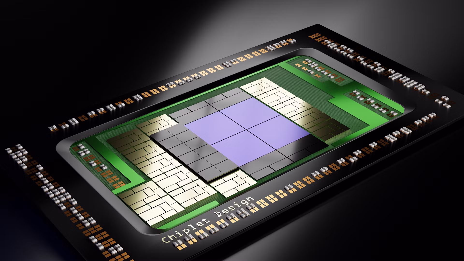
3D IC technology offers a compact and high-performance packaging solution that vertically stacks active dies using through-silicon vias (TSVs). This dramatically shortens interconnect lengths and enables heterogeneous integration of logic, memory, and analog elements in a tight footprint.
Ideal use cases include:
- AI and ML accelerators
- Demand tight coupling of compute and memory
- Require ultra-low latency and high bandwidth
- Benefit from logic-on-memory stacking for edge AI and inference workloads
- Mobile SoCs
- Require ultra-compact design with maximum performance
- Integrate CPUs, GPUs, modems, and memory in a single stack
- Crucial for smartphones, AR/VR devices, and wearables
- High-Performance Computing (HPC) systems
- Need high density and power-efficient compute performance
- Benefit from reduced power and footprint in datacenter and exascale systems
- Used in GPUs, CPUs, and specialized compute architectures
📌 Key advantage: Exceptional performance-per-watt and integration density for space-constrained or performance-critical systems.
Siemens EDA solutions for advanced IC packaging
Designing either 2.5D or 3D IC systems requires a unified toolchain that spans architecture, layout, verification, and test. Siemens EDA offers a full suite of solutions optimized for advanced packaging:
- Innovator3D IC™: Architectural exploration and interposer co-design
- Calibre® 3DSTACK: DRC/LVS and 3D signoff across stacked dies
- Calibre® 3DThermal: Accurate thermal analysis and modeling of 2.5D and 3D ICs
- Calibre® PERC™: Reliability verification for multi-die systems, including ESD and power integrity checks
- Aprisa™: Digital place and route with 3D-aware optimization for high-performance, multi-die designs
- Questa® Formal Pro: Formal verification to ensure functional correctness in complex 3D IC architectures
- Tessent® Multi-die: Test and yield strategies for stacked die systems
- 3D IC Packaging Resource Hub: Webinars, white papers, and technical deep dives
💡 Ready to evaluate these tools hands-on? Try Siemens EDA solutions with a free trial
Frequently Asked Questions (FAQ)
Q: What is the difference between 2.5D and 3D IC packaging?
A: 2.5D ICs place chips side-by-side on an interposer, while 3D ICs stack chips vertically using TSVs. 3D ICs offer higher performance, but 2.5D ICs are often more cost-effective and thermally manageable.
Q: Which is better for AI workloads—2.5D or 3D IC?
A: 3D IC is better suited for AI workloads due to its lower latency, higher bandwidth, and ability to stack memory directly on compute logic.
Q: Can I reuse chiplets more easily in 2.5D IC?
A: Yes. 2.5D systems often support greater modularity and reuse of dies across product generations.
Q: What Siemens tools help with advanced IC packaging?
A: Siemens offers Calibre 3DSTACK for verification, Innovator3D IC for prototyping, planning and co-design, and Tessent Multi-die for test insertion—plus a full resource library.
Final thoughts on choosing between 2.5D and 3D IC technologies
The decision between 2.5D and 3D IC technologies is not one-size-fits-all—it hinges on the specific requirements of your product and your broader go-to-market strategy. Power consumption, thermal constraints, form factor limitations, data bandwidth, and performance-per-watt targets all play crucial roles in determining the optimal packaging approach.
- If your design needs modularity, simplified thermal management, and rapid prototyping, 2.5D IC may offer the right balance of performance and manufacturability.
- For highly integrated systems demanding extreme density and efficiency—like AI accelerators, mobile SoCs, or HPC workloads—3D IC is likely the better choice, despite its higher complexity.
Both approaches represent a leap forward from traditional monolithic designs and are central to the future of semiconductor innovation.
At Siemens EDA, we help engineers and architects confidently navigate these decisions. Whether you’re new to multi-die integration or scaling an advanced 3D IC program, our comprehensive suite of tools, documentation, and resources supports every phase of the journey—from feasibility analysis to full silicon implementation.
🔍 Start exploring the possibilities:
- ✅ Try our IC packaging tools for free to evaluate real workflows with real data
- 📚 Browse our 3D IC resource library for whitepapers, case studies, and technical guides
- 🧠 Want a deeper dive into how to select the right packaging strategy?
👉 Read: Chip Packaging—Basics to Advanced 3D IC - 🔗 Read: 3D IC Guide to Heterogeneous Integration for real-world guidance on building next-gen systems
With the right strategy and the right partner, your 2.5D or 3D IC project can move from concept to tape-out faster, with greater confidence and performance gains. Siemens EDA is here to help you make it happen.
Tune into the 3D IC Podcast to learn from leading experts
🎙️ Curious about real-world applications and expert insights into 3D IC innovation?
Tune into the 3D IC Podcast to hear from engineers, product leaders, and semiconductor veterans shaping the future of advanced packaging.
Listen now on:


