Chip packaging explained: From IC packaging basics to advanced 2.5D and 3D IC technologies
Understanding the evolution and importance of chip packaging
As semiconductor innovation pushes the boundaries of performance and power efficiency, chip packaging—also known as IC packaging—has transformed from a back-end afterthought into a key enabler of system-level design. In today’s era of heterogeneous integration, advanced chip packaging technologies are at the forefront of enabling smaller form factors, faster data rates, lower power consumption, and higher system reliability.
In this article, we’ll walk through the basics of chip packaging, explore emerging trends, and highlight cutting-edge solutions that are helping design teams meet the growing demands of complex system-on-chip (SoC) and system-in-package (SiP) architectures.
What Is chip packaging?
Chip packaging refers to the protective casing that houses a silicon die, allowing it to interface electrically and thermally with the outside world. The packaging process not only safeguards the die from physical damage and contamination, but also plays a vital role in heat dissipation, electrical performance, and signal integrity.
Basic components of IC packaging include:
- Die attach materials
- Wire bonds or flip-chip interconnects
- Substrates
- Encapsulation and sealing compounds
As demand for higher performance, greater data capacity, and increased throughput has grown, the limitations of monolithic integration—particularly in terms of cost, yield, and manufacturing complexity—have driven a shift toward disaggregating functions into chiplets. These chiplets are then heterogeneously integrated within multi-die 2.5D and 3D IC configurations using advanced packaging platforms.
Traditional vs. advanced IC packaging approaches
| Packaging Type | Description | Use Cases |
| Wire Bonding | Oldest and most cost-effective packaging method, using thin wires to connect the die to the substrate. Best suited for low pin count applications where performance is not a critical requirement. Despite its limitations, wire bonding remains widely used, packaging roughly 90% of ICs today. | Legacy analog, power management, and low-performance applications |
| Flip-Chip Packaging | Uses solder bumps placed directly on the die, which is then flipped onto the substrate. This shortens interconnect paths, reducing inductance and improving electrical performance, thermal dissipation, and reliability—ideal for high-density and high-performance requirements | Microprocessors, memory devices, image sensors, and high-frequency ICs where performance, interconnect density, and reliability are critical |
| System-in-Package (SiP) | Integrates multiple fully functional ICs and passive components into a single compact package to create a complete electronic system. Unlike modern 2.5D and 3D ICs that often use disaggregated chiplets with partial functionality, traditional SiPs combine complete subsystems | Wearables, smartphones, IoT devices, medical electronics, and automotive systems where space, power efficiency, and functionality integration are key |
| Fan-Out Wafer-Level Packaging (FOWLP) | An advanced packaging technology that extends I/O pads beyond the die footprint by embedding the die in a reconstituted wafer and using a redistribution layer (RDL). This eliminates the need for an interposer or substrate, resulting in a thinner package with improved electrical and thermal performance | Mobile SoCs, RF modules, power management ICs, and high-performance computing where small form factor, high I/O density, and thermal efficiency are essential |
| 2.5D and 3D IC Packaging | Stacks or places dies side-by-side using silicon interposers or TSVs for high bandwidth and integration | AI/ML processors, HPC, data centers |
To design for these advanced packaging techniques, specialized EDA tools are required to handle layout complexity, signal integrity, and thermal reliability. Siemens’ IC Packaging solutions enable designers to manage these challenges from concept to signoff.
The rise of heterogeneous integration and 3D IC
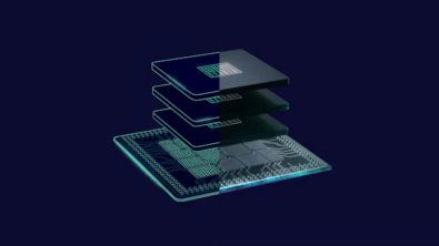
Driven by the need to integrate more functionality into increasingly compact form factors, advanced packaging technologies like 3D IC and heterogeneous integration are transforming the landscape of chip design. While traditional System-in-Package (SiP) approaches integrate fully functional dies—such as logic, memory, RF, and analog—into a single package, 2.5D and 3D IC architectures go further by enabling the integration of chiplets, often with partial functionality, across multiple process nodes. True 3D ICs, which feature vertically stacked and directly interconnected dies, are sometimes referred to as System on IC (SoIC), reflecting a new level of integration density and performance.
What is 3D IC packaging?
As semiconductor packaging evolves from traditional approaches to advanced architectures, 3D IC packaging plays a key role. It refers to the vertical stacking of semiconductor dies within a single package to improve performance, reduce footprint and increase bandwidth.
Benefits of 3D IC packaging:
- Increased performance through tight integration and reduced signal delays
- Reduced power consumption thanks to shorter interconnects and lower parasitic losses
- Dramatic increase in bandwidth enabled by high-density vertical interconnects
- Heterogeneous integration of logic, memory, RF, and analog dies from different process nodes or foundries
- Improved electrical performance due to lower inductance and resistance
- Smaller form factor ideal for space-constrained applications
- More efficient use of space with vertical stacking of dies
- Enhanced system capability by combining specialized functions in a single package
- Greater design flexibility for creating application-specific, high-performance systems
However, 3D IC design introduces new challenges in areas like power delivery, thermal management, and design rule checking. Siemens offers a comprehensive 3D IC design platform that supports full-system co-design, enabling faster iteration and first-pass success. For a deeper look at how 3D IC systems are designed and verified end-to-end, see the 3D IC guide to heterogeneous integration.
Meeting the verification challenge: DRC, LVS, and beyond
As semiconductor designs evolve toward advanced 2.5D and 3D IC packaging architectures, verification becomes significantly more complex. Traditional Design Rule Checking (DRC) and Layout Versus Schematic (LVS) methodologies—while effective for monolithic SoCs—struggle to address the intricacies introduced by multi-die integration. In 3D ICs, designers must contend with new physical interactions such as vertical interconnects, microbumps, through-silicon vias (TSVs), and interposers, which introduce novel parasitic effects and demand more comprehensive rule enforcement across dies and packaging layers.
- DRC must now validate not only lateral spacing and geometries within a single die, but also cross-die connectivity and alignment, inter-die bump placement, and wafer-level stacking constraints.
- LVS, on the other hand, faces the added complexity of verifying connectivity across disparate dies—each potentially designed in a different technology node or by different teams—while ensuring electrical consistency with the top-level system schematic.
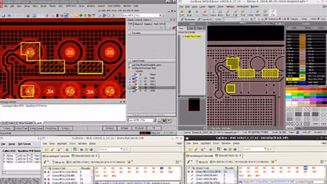
To meet these multifaceted verification needs, the Calibre® 3DSTACK platform from Siemens EDA extends the industry-leading Calibre signoff capabilities into the 3D IC domain. It enables silicon-accurate physical verification for advanced packaging by incorporating hierarchical, multi-domain DRC and LVS that span across chiplets, interposers, and redistribution layers. Foundry-qualified rule decks ensure that designs adhere to manufacturing constraints, while robust 3D inter-die checks validate alignment, connectivity, and parasitic impacts—giving engineers full signoff confidence at system scale.
Innovating faster with integrated design environments
To truly accelerate design cycles, IC packaging teams benefit from unified, collaborative design environments. Siemens’ Innovator 3D IC empowers multi-disciplinary teams to concurrently co-design across logic, package, and board domains—cutting down cycle time and enabling rapid prototyping.
With integrated thermal, mechanical, and electrical analysis, engineers can quickly optimize tradeoffs and reduce the risk of late-stage failures.
Key considerations when choosing a chip packaging strategy
When selecting a packaging solution for your design, consider the following:
- Thermal performance requirements
- Signal and power integrity needs
- Interconnect density
- Manufacturing costs and supply chain
- Time-to-market pressures
Not every application demands the most advanced packaging. A holistic understanding of system-level goals helps teams determine whether wire bonding, flip-chip, or 3D IC is the right fit.
Frequently asked questions about chip packaging
What is the difference between chip packaging and IC packaging?
These terms are often used interchangeably. Chip packaging refers broadly to the encapsulation and interfacing of a semiconductor die, while IC packaging typically refers to packaging for integrated circuits, which are specific types of chips. Both involve similar technologies and challenges.
Why is advanced chip packaging important?
As Moore’s Law slows, performance gains are increasingly realized through architectural innovation. Advanced chip packaging allows integration of multiple dies, improving bandwidth, lowering power, and enabling heterogeneous systems.
What tools are required for 3D IC packaging?
Designing for 3D IC requires tools for layout planning, thermal/electrical analysis, and verification. Siemens’ 3D IC design solution and Calibre 3D IC verification platform provide end-to-end support for these needs.
How do I get started with advanced IC packaging?
Start by understanding your system’s performance and integration goals. Explore collaborative design tools like Siemens’ technology to enable concurrent development across disciplines.
Conclusion: chip packaging as a strategic advantage
Modern chip packaging is no longer a passive step in the semiconductor lifecycle. It’s a strategic enabler of next-gen performance, especially in AI, HPC, and mobile computing. As packaging complexity grows, design teams must adopt intelligent workflows and integrated tools to stay competitive.
To learn more about how Siemens EDA can help you simplify and accelerate your IC packaging process, explore our complete IC packaging solutions.
🎧 Curious about where 3D IC technology is headed?
Tune into our “3D IC” podcast series, where industry experts and innovators unpack the trends, challenges, and breakthroughs shaping the future of advanced IC packaging. From chiplet architectures to thermal and signal integrity in stacked designs, each episode delivers actionable insights for engineers, designers, and technologists navigating the evolving semiconductor landscape.
Join host John McMillan and a lineup of thought leaders as they explore how 3D IC is redefining performance, power efficiency, and integration strategies.
Helpful internal links for further exploration:
- 3D IC technology: your comprehensive guide to enabling heterogeneous integration
- Siemens IC Packaging Overview
- 3D IC Design Solutions
- Innovator 3D IC Technology
- Calibre 3D IC for Design Verification


