A deep dive into HDAP LVS/LVL verification
Today, EDA companies are developing tools and workflows to support HDAP (High-density advanced packaging) LVS/LVL verification. Though the data for achieving “signoff-level” confidence is a work in progress, EDA companies are providing tools that can adapt to different levels of data availability and enable HDAP designers to execute HDAP LVS/LVL flows that are both productive and beneficial.
Why is verification for HDAP designs such a challenge?
The reality is, HDAP designs are now real products. For the past decade, all variations of HDAP technologies promised an improved form factor and functionality by integrating multiple integrated circuit (IC) dies built using different technology nodes (heterogeneous integration). Figure 1 shows the two most popular HDAP technologies—2.5D (interposer) and fan-out wafer-level packaging (FOWLP) designs.
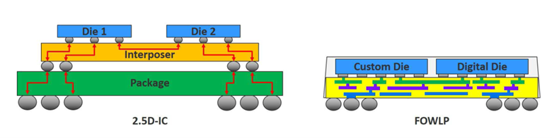
Figure 1
Verifying HDAP designs is necessary to ensure their intended performance and reliable in mass production to meet market demand. However, the EDA industry has faced challenges in automating HDAP verification because it involves combining IC and package verification components. Considerable time and effort have been devoted to identifying the issues and proposing or developing solutions. For example, the overall idea of qualified assembly design kits (ADKs) resembling IC process design kits (PDKs) has begun to materialize to some extent – and at least one EDA solution now enables assembly-level LVS verification for HDAP. Notably, the importance of post-layout simulation for analog and post-layout static timing analysis for digital HDAP designs is widely acknowledged.
How mature is HDAP physical verification?
The quick answer is: It’s a work in progress. After design, the natural first step is the physical verification of the HDAP design. These HDAP designs contain multiple heterogeneous dies connected through a package and while each die in the HDAP has been functionally verified by itself – you MUST ensure that the entire HDAP functions as expected after manufacturing. Although HDAP design company flows continue to mature, there is still quite a lot for EDA companies, foundries/OSATs, and HDAP design companies to learn.
How can you ensure verification data completeness?
Consider LVS verification for an HDAP design for example – an SoC can’t be approved for manufacturing unless the geometries built in the layout design implement the connectivity required by the original schematic/design intent. LVS verification is a mature, well-established, automated flow in the SoC world. EDA LVS tools for SoCs require a consistent set of basic inputs:
- Layout database (format can be GDSII, OASIS, or LEF/DEF)
- Source netlist (format can be SPICE or Verilog)
- LVS rule deck (format based on the EDA company’s proprietary syntax)
Looking at HDAP LVS verification, we can identify major differences. The most obvious and critical is that design companies, foundries/OSATs, and EDA companies are not in alignment or agreement on the set of inputs required for an HDAP LVS flow. This disconnect exists for three reasons: ownership, data availability, and design dependence.
- Ownership – Because HDAP is still an emerging technology, the responsibility for HDAP verification can often end up with different teams in different companies.
- Data availability – To enable LVS verification of an entire HDAP, all the data for all the components must be available.
- Design dependence – In SoC LVS verification, the LVS rules deck is only dependent on the SoC technology node information. HDAP LVS adds another complexity: die placements. An HDAP LVS rule deck is dependent on the GDSII layers of the interposer, die1, die2, etc., but it is also dependent on where the dies are placed. In turn, this information is highly dependent on the HDAP design itself.
What does LVS verification look like in different flows?
It’s not practical for EDA companies to enforce a certain set of data requirements for HDAP verification. EDA companies must be flexible, in that there should always be some type of HDAP LVS verification that can be achieved with the available data.
What LVS verification might look like in different flows for different cases:
- Package/interposer connectivity checking without a schematic/design intent: The concept of a “source netlist” in a standard format is relatively new in the packaging world.
- Package/interposer LVS without die pins: This case presents a more advanced situation in which the verification data now includes both a package design database and a source netlist, so designers should be able to run a true LVS verification.
- Assembly-level LVS/LVL: LVL verification is equally as important as LVS in HDAPs, especially when rotation or scaling is required. Designers must ensure that, after processing, there is still sufficient overlap between the package bumps and die bumps. Overlaps include both Geometrical die interface only and Geometrical die interface + logical die pins.
As HDAP technologies become mainstream, HDAP designers require reliable design and verification flows from both foundries/OSATs and EDA companies. However, the HDAP verification flows currently available are far from mature when compared to traditional, well-established SoC verification flows. Thus, EDA companies must provide tools and flows that can account for various levels of data availability, while still enabling HDAP designers to perform useful and valuable HDAP LVS flows.
To learn more, download this whitepaper written by Tarek Ramadan, 3D IC Technical Team Leader at Siemens EDA entitled “A deep dive into HDAP LVS/LVL verification” which addresses the questions posed in this blog as well as provides detailed insights on the path to verification completeness.
Click here to learn how you can deliver product differentiation faster using 3D heterogeneous integration of node and performance-optimized chiplets with Siemens EDA’s market-leading 3D IC technology solution.
Want to learn more about 3D IC technology?
- Listen to The future of semiconductor design podcast, in which industry experts discuss 3D IC concepts and the latest trends: chiplet designs, IC packaging, multi-die verification, golden netlists, electrical signoff, system analysis, and more!
- Read The beginner’s guide to 3D IC to discover how 3D IC is evolving.
- View this infographic to learn how to Unlock the potential of 3D IC.
- Learn more about 3D IC front-end design planning and predictive analysis in this ebook entitled “Launching the full potential of 3D IC with front-end architectural planning” to
- Discover the 3D IC design workflows available to designers in this eBook entitled: Semiconductor packaging: making the right connections in 3D IC design


