The beginner’s guide to 3D IC
Why 3D IC technology matters
As consumer electronic devices grow increasingly connected, intelligent, and advanced, designers need new methodologies like 3D IC to address “More-than-Moore” limitations. These increasingly complex devices include more features and intricate circuit designs, demanding higher processing capabilities. To keep pace, engineers require new strategies for designing and integrating chips, and 3D IC technology delivers that breakthrough.
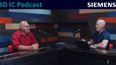
If you prefer video to text, watch this 22-minute Introduction to 3D IC Podcast Episode. You’ll learn the fundamentals of 3D IC, key adoption trends, and engineering challenges.
We know everyone has their own learning style—whether you read the guide below or watch the episode, we hope this helps you better understand 3D IC technology.
What is 3D IC?
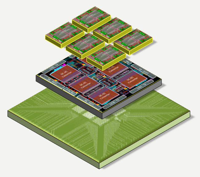
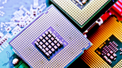
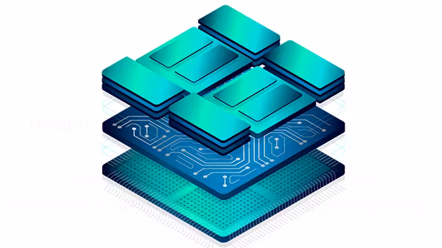
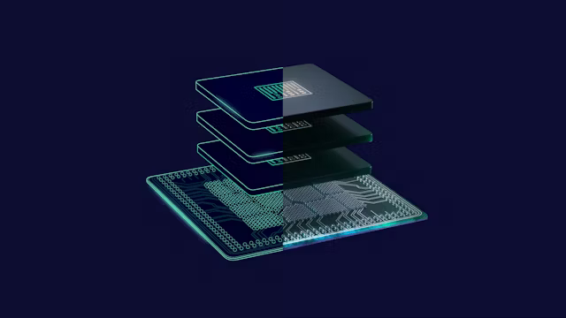
A 3D IC is a three-dimensional integrated circuit that encompasses both the integration strategy and enabling technologies. In 3D IC designs, traditional monolithic SoCs are disaggregated into smaller functional chips or “chiplets,” integrated within a high-performance package. These vertically integrated systems deliver significantly higher performance and consume less space than conventional monolithic chips.
A notable early example of stacked integration is High Bandwidth Memory (HBM), introduced roughly a decade ago. Stacked memory dies dramatically increased density within a small footprint and were integrated alongside ASICs using 2.5D interposer technology—where the term originated.
💡Learn more about how chiplets enable advanced integration in 3D IC Guide to Heterogeneous Integration.
Why the semiconductor industry is moving toward 3D IC
The shift toward 3D IC is driven by the need to overcome fundamental limitations of traditional semiconductor scaling and packaging approaches. 3D IC technology enables:
- Power Efficiency: Traditional system-on-chip (SoC) designs require long interconnects that consume significant power, particularly as clock frequencies and bandwidth demands increase. In 3D IC architectures, shorter interconnects between vertically stacked dies reduce resistive losses, lower overall power consumption, and improve energy efficiency—a critical factor for mobile devices, wearables, and battery-powered electronics.
- Performance Gains: Advanced applications such as AI, HPC, and 5G require exceptional bandwidth and low-latency interconnections between compute and memory elements. 3D IC allows designers to place memory and logic dies in close proximity, dramatically boosting data transfer rates, reducing signal delays, and supporting high-speed system performance.
- Form Factor Reduction: With conventional monolithic designs, there’s a practical limit to chip size—determined by photomask reticle size, typically around 25 to 27 mm per side. 3D IC circumvents this restriction by stacking dies, significantly shrinking the overall footprint while expanding functionality. This space-saving approach is ideal for mobile devices, IoT sensors, and edge computing systems where compactness is essential.
- Heterogeneous Integration: Integrating all system functionality onto a single die often requires compromises in process technology. With 3D IC, designers can implement chiplets using different, highly specialized process nodes tailored to each function—whether logic, memory, analog, RF, or photonics. This flexibility enables performance optimization, cost efficiency, and improved yield across complex designs.
In short, 3D IC eliminates constraints around chip size, process uniformity, and integration complexity—allowing engineers to build larger, higher-performance, more capable systems that were previously unattainable using traditional SoC methods.
🔎For a full overview of packaging approaches, read Chip Packaging—Basics to Advanced 3D IC.
2.5D vs. 3D IC: what’s the difference?
While both technologies advance semiconductor packaging, understanding the differences is critical for selecting the right approach:
- 2.5D IC: Multiple dies are placed side-by-side on a silicon or organic interposer—a passive layer that provides lateral interconnections between chiplets. This allows for integrating heterogeneous components, like memory, logic, and analog dies, with high-bandwidth, short-reach connections, while simplifying thermal management compared to stacked designs.
- 3D IC: Dies are stacked vertically using Through-Silicon Vias (TSVs) or advanced hybrid bonding techniques for direct die-to-die communication. This enables the highest interconnect density and shortest signal paths, improving performance, reducing power consumption, and shrinking form factors. True 3D IC allows designers to partition large, complex systems into multiple vertically integrated layers, overcoming die size limitations and boosting computational density.
Compared to traditional Multi-Chip Modules (MCMs), both 2.5D and 3D IC architectures provide superior system integration. However, 3D IC achieves:
- Greater interconnect density and bandwidth
- Significantly reduced wiring length and signal latency
- Improved system performance and energy efficiency
- The smallest possible physical footprint for high-complexity systems
Choosing between 2.5D and 3D depends on the application’s power, performance, thermal, and integration requirements. Many high-performance systems use a hybrid approach, leveraging both 2.5D interposers and 3D stacking within the same package.
For a deeper dive into this topic, explore our in-depth guide comparing 2.5D vs. 3D IC approaches: Chip Packaging—Basics to Advanced 3D IC.
Key applications of 3D IC technology
3D IC integration powers innovation across industries:
- High-Performance Computing (HPC): 3D IC enables ultra-high bandwidth, energy-efficient systems that meet the extreme performance demands of data-intensive workloads in scientific research, simulation, and advanced analytics.
- AI and Machine Learning Accelerators: Stacking compute and memory elements with minimal signal delay accelerates training and inference processes for artificial intelligence applications, boosting processing speed and energy efficiency.
- 5G and Wireless Infrastructure: 3D IC supports the dense, compact system designs required for 5G base stations, small cells, and network equipment, delivering faster data rates, lower latency, and improved connectivity.
- Data Centers and Cloud Computing: Vertically integrated chiplets increase processing density and reduce power consumption, critical for optimizing performance-per-watt in hyperscale data centers and edge servers.
- Consumer Electronics and Mobile Devices: Smartphones, tablets, wearables, and AR/VR devices benefit from 3D IC’s ability to integrate more functionality into smaller form factors while enhancing battery life and performance.
- Automotive and Advanced Driver-Assistance Systems (ADAS): The combination of compact size, heterogeneous integration, and high reliability makes 3D IC ideal for sensor fusion, real-time decision-making, and compute-heavy tasks in next-generation vehicles.
As semiconductor complexity increases, 3D IC is playing a pivotal role in delivering performance, power efficiency, and miniaturization across these critical application domains.
Overcoming 3D IC design challenges
While 3D IC technology provides remarkable advantages, it presents engineering hurdles:
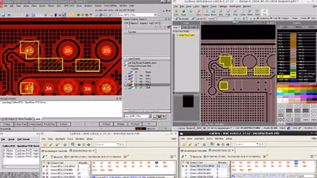
- Thermal Management: Designers must manage complex power profiles across multiple stacked dies. Tools like Calibre 3D Thermal Analysis help predict thermal behavior.
- Mechanical Stress Analysis: Die stacking and substrate differences introduce stress risks. Simulation tools model mechanical impacts to prevent failures.
- Power Delivery Network Design: Multiple chiplets with varying voltage and noise requirements increase PDN complexity.
- Test and Yield Optimization: Testing interfaces between chiplets requires advanced methodologies such as Tessent Multi-die Test.
- System Design Complexity: Integrating chiplets demands robust tools for placement, routing, and signoff, including Calibre 3D IC Verification and Aprisa Physical Design and Innovator3D IC.
The role of EDA tools in 3D IC development
Electronic Design Automation (EDA) tools are essential for realizing 3D IC innovation. With the complexity of multi-die integration, stacking, and advanced packaging, manual design approaches are no longer feasible.
Siemens EDA delivers comprehensive solutions that support the entire 3D IC development flow:
- 3D IC Design Planning and Packaging: Tools for system-level planning, partitioning, and integrating heterogeneous chiplets into optimized packages, including support for silicon interposers, organic substrates, and advanced stacking techniques.
- Thermal, Stress, and Reliability Analysis: Simulation solutions to model heat distribution, mechanical deformation, and long-term reliability risks to ensure robust system performance.
- Multi-Die System Verification and Signoff: Electrical, physical, and functional verification of complex multi-die assemblies, enabling first-pass design success and manufacturability.
- High-Density Interconnect Optimization: Design and analysis tools to implement ultra-short, low-resistance interconnects between stacked or side-by-side chiplets, maximizing bandwidth and energy efficiency.
- Test, Yield, and Manufacturability Improvement: Integrated methodologies for wafer-level test, die-level test, and package-level system test, ensuring product quality, high yield, and production scalability.
- 3D Integration-Aware Physical Design: Floorplanning, routing, and placement tools optimized for stacked die environments, enabling higher density and performance.
Learn how to accelerate development and manage complexity with Siemens Innovator3D IC.
Frequently Asked Questions (FAQs)
What is the difference between 2.5D and 3D IC?
2.5D IC uses lateral placement on an interposer, while 3D IC stacks dies vertically, providing greater integration density and performance. Learn more: Chip Packaging—Basics to Advanced 3D IC
Why are 3D ICs critical for AI and HPC?
3D IC enables the bandwidth, low latency, and compute density needed for AI accelerators and high-performance computing systems.
What challenges do designers face with 3D IC?
Thermal management, mechanical stress, complex power networks, and testability are major challenges. Advanced tools mitigate these risks.
How does hybrid bonding enhance 3D IC?
Hybrid bonding creates high-density, low-resistance connections between stacked dies, improving performance and reliability—sometimes replacing TSVs.
Where can I learn more?
Visit Siemens 3D IC Design, Innovator3D IC, and dive deeper with our 3D IC Guide to Heterogeneous Integration.
3D IC is driving semiconductor innovation
As Moore’s Law slows, 3D IC provides new pathways for performance scaling, system miniaturization, and heterogeneous integration. Whether you’re an engineer, product manager, or technologist, mastering 3D IC concepts is essential for advancing semiconductor design.
With proven solutions like Innovator3D IC, Calibre 3D IC, Aprisa, and Tessent Multi-die Test, Siemens empowers innovators to overcome design complexity and bring next-generation 3D IC products to life.
Explore more at Siemens 3D IC Packaging.
🔍 Start exploring the possibilities:
✅ Try our IC packaging tools for free to evaluate real workflows with real data
📚 Browse our 3D IC resource library for whitepapers, case studies, and technical guides
🧠 Want a deeper dive into packaging strategy?
👉 Read: Chip Packaging—Basics to Advanced 3D IC
🔗 Read: 3D IC Guide to Heterogeneous Integration for practical system design insights
Want to learn more about 3D IC? Listen to the podcast now, available on your favorite podcast platform.
View the episode transcript
[00:10] John McMillian: Welcome to the Siemens EDA podcast series on 3D IC Heterogeneous Integration brought to you by the Siemens Thought Leadership team. I’m your host John McMillian. If you’re involved in any form of semiconductor and semiconductor packaging design, you will have seen and/or heard the term “3D IC” being broadly discussed and promoted. 3D IC is often referred to as a path to “more than Moore;” a reference to Gordon Moore’s observation that the number of transistors on a semiconductor doubles every two years, and along with that, the associated speed, capacity, and throughput. Another tenet of this so-called Moore’s Law asserts that this growth is exponential; however, experts agree that semiconductors may be close to reaching their physical limits due to multiple technical and technology reasons, as well as business and/or marketing reasons. This has led to design teams turning to the disaggregation of once monolithic implementation architectures into several smaller functional chips or chiplets, which are then reaggregated or integrated using a high-performance package. 3D IC refers to an integration, methodology, and technology.
[01:19] John McMillian: Today, in our first podcast in a four-part series, we are discussing what 3D IC integration technology is? And what exactly is driving it and why? I’m pleased to introduce my special guest, Anthony Mastroianni, who is the 3D IC Solutions Architect Director at Siemens Digital Industries Software. Welcome, Tony. And thank you for taking the time to talk with me today about 3D IC. And before we dive into the discussion, would you mind giving our listeners a brief description of your current role and background?
[01:49] Tony Mastroianni: Sure, John. Thank you for the intro, I’d be happy to do that. Again, my name is Tony Mastroianni. And I’ve been in the semiconductor industry for over 30 years. I’ve been involved primarily in the design of custom integrated circuits. Most of that time, in the role of a design manager. I worked for Semiconductor for the last 18 years. And in the last three or four years in that role, we started getting involved in working on two-and-a-half D designs that were using HBM memories for some very complex systems, processors, as well as 5G base station controllers. It became evident, as we started doing those complex two-and-a-half D designs, that our packaging methodology did require some considerable overhauls and improvements. So, I spent the last couple of years working and modifying our two-and-a-half D design process. The company I was with was acquired last year in 2020. I started with Siemens, and they’ve asked me to drive their advanced packaging design strategy and methodology. So, what I’m focusing on are complete solutions and workflows for two-and-a-half and 3D IC solutions, as opposed to just providing point solutions. That’s my primary role here at Siemens.
[03:20] Tony Mastroianni: So, I’d like to talk a little bit about what’s happening in the semiconductor in the design and the packaging space that’s kind of driving this 3D IC. What’s happened due to Moore’s law is the ASIC technology has been advancing over the last 40 years or so. And we’re getting to a point where the level of device scaling, it’s taking longer to make smaller transistors. And the costs are becoming extremely high for these technologies and the design, analysis, as well as the manufacturing of these chips. So, the advanced ASIC technology nodes, over the past 40 years, the transistors have scaled dramatically and the performance has also increased. But as we’re approaching the end of Moore’s law, the rate at which the devices are shrinking is reduced. It’s taking longer and the cost is going up dramatically. Another thing is HBM memories, these are high bandwidth memories. This is some technology that came out about 10 years ago, where multiple memory chips are stacked on top of each other to give you a tremendous amount of memory in a very small footprint. And that’s put into an unpackaged device, and that gets integrated into AISC on a two and a half d interposer. So that’s that’s where we come with the term “two-and-a-half d.” And it started really with HBM memory, so that really kind of drove this methodology. And that’s been around for about 10 years or so.
[04:55] Tony Mastroianni: Now again, due to Moore’s law, we’re hitting a limit; the transistor scaling is reduced. And there are practical limitations on how large you can make a device. And it’s really limited by what’s called the photomask and a reticle size, and that’s basically the maximum size that a chip can be. And it’s on the order of 25 to 27 millimeters on a side. So you really cannot make a chip larger than that, physically. Since the number of transistors scaling has reduced, we’re not getting the benefits of increased complexity by putting more and more devices into a single package. Another issue is intellectual property. So, an SOC, or System On Chip, intellectual property are the basic building blocks that are implemented in that chip. And this may be high-performance IO, such as, it may be PCI Express interfaces, HBM memory interfaces, and such. As some of these types of functions do require very specialized ASIC technologies, in some cases, it could limit what you can implement in the system because you would need all the IP available in the same process if you’re going to integrate that into a single chip. When we get into 3D IC, you no longer have that limitation. So, you can acquire chiplets, which perform a certain function, let’s call it intellectual property. That chiplet can be optimized using the technology which is most appropriate for that type of functionality.
[06:38] Tony Mastroianni: So, I talked about the device scaling. So, by not being limited to how large a device it can be, we really can create much larger systems by putting multiple chips in a package. So, the implications of monolithic design for certain products such as high-performance compute and AI devices will still continue to use monolithic technologies. But they could actually leverage from some of this disaggregation by perhaps splitting the design up into a smaller set of chips. But in general, if you can fit everything you need in a single chip, you will get the lowest unit cost and the highest performance. But when you hit some of those limitations, that’s where two-and-a-half D or 3D technologies can allow us to extend the capabilities of these systems.
[07:29] John McMillian: So there are a considerable number of growing pressures on traditional monolithic design. Can you tell us what approaches semiconductors teams have been adopting to achieving a device’s functionality goals?
[07:42] Tony Mastroianni:Sure. When we talk about putting multiple chiplets or chips into a package, there’s several different underlying technologies. People have been designing multi chip modules for many, many years, and that’s essentially putting one or more ASIC chips into a single package, and then connecting those with traditional packaging technologies. So, that’s referred to as an MCM module. There are many different technologies. And that’s a very mature technology but there are some limitations of that. So, when we get into 3D IC, this is really being driven by much more advanced packaging technology that allow you to integrate what I call chiplets. And a chiplet really is an ASIC that’s been designed to be integrated with other chiplets within a package. And there really are two general classes: 2D and 3D. We use the term “two-and-a-half D,” and that really came from the fact that we’re integrating a 3D HBM memory along with another ASIC. So, it really is 2D integration; you’re just integrating two chips on a single interposer – it may be organic or silicone. And then you’re interconnecting those chiplets on that interposer using metal interconnect. The other class is 3D. And that kind of falls into two different categories. One of them is Die Stacking. And there are really kind of two general applications that are being deployed today. One of them is stacking memory on top of a chip in one application that AMD and Intel and companies developing very large complex processor, they’re actually decomposing those processors into smaller building blocks. And then they’re actually taking some of the cache memories out of the die, and putting those in a separate die, and stacking that on top of the processor die. So, that’s what we call 3D. And in this case, it’s really just taking some of the functionality – maybe a memory – and putting that on top of the functional chip and then connecting those using the 3D packaging technology.
[09:56] Tony Mastroianni: Another application of Die Stacking would be in sensor type applications where you may have sensors that are gathering photo sensors or whatever. And then that sensor chip would be stacked on top of, say, a memory chip. So you would take that sensed data, store it to memory, and then maybe that would be stacked on top of a processing type trip. That’s what we call Die Stacking. Now, True 3D is a term where you’re actually taking an ASIC, and you have the ability to actually split that ASIC into two chips and stack them on top of each other. So, this requires the ASIC place-and-route tools to have the ability to not only place the logic in a traditional 2D manner on a chip, but now it can actually decide to partition some of the logic in one die that stacked on top of another or below another. So, this is really a very advanced methodology that will have some tremendous performance benefits. But it really is a newer technology, it is much more complex, so it’s really not really in production today. Whereas the other methodologies that I just mentioned are in production today.
[11:15] John McMillian: So, semiconductor design teams, they already have quite a range of choices to counter, some of the monolithic challenges. But as you point out, none of them seem to be a “one size fits all” or silver bullet, which I guess is why 3D IC integration is emerging. Please explain what 3D IC integration is and why it’s technically different from the other technologies we just discussed.
[11:36] Tony Mastroianni: So, what we’re talking about is putting multiple chips in a package. And primarily, the difference between the traditional MCM is the packaging technology – so that may be either 2D or 3D. And the key difference there is the interconnect between those devices is really being implemented at the silicon level. So, the geometries are considerably smaller. Since the wires essentially are much shorter and thinner, the resistance and capacitance is considerably slower. So that gives you the benefits that you can implement significantly more connections between those chips. And also you have much less parasitics, which means you can run them at much higher speeds. So, in effect, it is these packaging technologies, whether it be 3D or 2D, that offered the fine feature size of this interconnect enables increased performance that allows you to do much more greater complexity – since you can do many more interconnects – and allows you to build systems with a much smaller footprint inside of a single package. So, systems, in effect, can be decomposed into functions that are implemented as smaller chips, or what we call chiplets, as opposed to putting everything into a single homogeneous ASIC device. The other difference here is system designers now have more options to implement their complex devices and take advantage of some of the inherent benefits of two-and-a-half and 3D. So it offers them more options in developing their systems, taking advantage of some of the benefits offered by these technologies.
[13:20] John McMillian: It makes it clear what 3D IC integration is and why it’s technologically different. Can you tell us what a device design goals and/or objectives would be that would make a 3D IC the right integration platform?
[13:34] Tony Mastroianni: Any design goal or objective, obviously, is going to be unique to the particular design that the system designer is trying to design. So, again, the benefits of two-and-a-half and 3D would need to be considered to see how those objectives and goals can be achieved. So, the benefits that we’re talking about through 3D IC integration are, again, since we have smaller wires, we have reduced latencies which gives us – in the example of HBM memories – much higher memory bandwidth access, so you get performance advantages here: higher speed, better memory throughput. Scalability – so, we do have some practical limitations on how large a device can be made. If we have the ability to split a chip up into smaller chiplets and integrate those on a larger interposer or stack them, we can scale our systems much more gracefully. Building an ASIC device takes considerable time, cost, and time to market. It takes anywhere from one to three years to develop a complex SOC. But by having these pre-built building blocks, if you will, and maybe a smaller, less complex ASIC built into a system and package; it gives us the ability to implement different options of the product. So we can scale the product and have different product configurations leveraging this technology. Considerably shorter time to market, as well as reduced costs because you’re using packaging technology as opposed to the very expensive IC technology that we talked about before.
[15:16] Tony Mastroianni: The size, obviously, is smaller as well. So, for the reasons we talked about, we can implement a smaller footprint that goes into whatever product, ultimately, this will be in, leveraging either the two-and-a-half or 3D technologies. And power also – since we are connecting these chips that are placed right next to each other, the distances are much shorter, so we can run those at higher speeds at lower power, as opposed to putting chips on a board which may be several inches or a foot or more. So, we do have lower power because we’re driving these high-speed signals at much shorter distances. And also the benefits of cost, and the cost can become reduced by having smaller die, which would give us a higher yield and a lower unit costs for those chiplet components as well as the [16:15 inaudible] because if we’re integrating IP into an ASIC, for example, let’s say, a 56-gigs [16:22 inaudible] that may be on the order of $10 million for that piece of IP to be integrated into an ASIC. Now, if you need that functionality and that can be acquired from a chiplet, you’re really just paying for the end results, you’re not really paying for the IP costs for that. So there can be considerable savings in both the unit cost as well as the non-recurring engineering cost in deploying some of these technologies.
[16:49] John McMillian: Those are very compelling points. So, now that we understand what 3D IC integration is and why it’s differentiated from other advanced integration packaging technologies. But, sure, there must be some challenges in moving into 3D IC.
[17:02] Tony Mastroianni: Of course, yeah, there’s no such thing as a free lunch. So, 3D IC does bring some challenges to the table. And we’ll talk about some of these. The first is really thermal. So, in designing a traditional ASIC device, that device will have a certain power profile. And then that power profile can be modeled. And then the package design really just needs to be able to deal with that simplified thermal power model. And historically, you could just analyze the package, make sure you have the ability to take that heat out of the chip and dissipate that and you’re done. But when you put multiple chips inside a package, that power profile becomes much more complex. So, you do need to, rather than just having a very simplified single model, you have to deal with multiple chiplets in each of the power and thermal profiles of all those chiplets.
[18:01] Tony Mastroianni: The other thing that you need to be concerned with is the thermal interaction between these different devices. So, one example might be, let’s say, an HBM memory which has an operating condition of at 85C, maybe sitting next to an ASIC that is designed to run at 125C. And if those devices are too close and you’re not careful, the SOC can actually heat up that memory and knock it out of spec. So, again, you have to analyze the thermal interaction between each of those components to make sure that you’re meeting the thermal requirements of the device. Another thing which is unique to two-and-a-half and 3D type designs is mechanical stress analysis. So, when you stack die or stack a large silicon interposer on top of an organic substrate, the thermal expansion coefficients between silicon and those organic materials are different, so they will bend and flex differently. And that can create some mechanical stress on the connections between those devices, which can cause failures and reliability issues. There are different design techniques that are used to deal with that. And really, since every design is unique, that analysis needs to be done with mechanical simulators to model that stress.
[19:25] Tony Mastroianni: One of the probably most complex issues that comes up in these technologies is the testability. So, testing a single device, that technology is very mature. And generally, it’s a two-step process. So, as the chips are manufactured, they get tested while they’re still on the wafer. This is called wafer-level testing. So, there are probe cards that go and test the device. And if they’re good, they’ll go through and then they’re just marked if they’re bad, so you don’t package up the bad devices. And then once it’s in the package, generally, you’re going to retest the package with the chip inside of it, that’s called the final test. Now, when we get into two-and-a-half and 3D devices, we have multiple chips that are inside that package. So, you do need to test the interfaces between each of those chips, you still need to retest those devices once they’re in the package. So, presumably, the chiplet providers have tested those before they ship those to their customers. So, they are wafer-tested before they’re delivered to the system integrators. But during the assembly process, it’s possible that they may have been damaged. So, there is a need to retest those devices. So, that would require the test patterns associated for those chiplets to be a deliverable provided from those chiplet vendors.
[20:50] Tony Mastroianni: The other issue is you don’t have access to all the pins for each of those chiplets. So, different test techniques and test tools and DFT tools are required to be able to test those two-and-a-half and 3D devices. Another issue is your power delivery network – designing and analyzing that network. So, multiple chiplets may have different voltage supplies and different power requirements, different noise requirements – so, that all needs to be considered during the package design process, and making sure that you’re delivering the power to each of those components and meeting the requirements of that. So, there are other issues, but I’d say these are the primary things that need to be addressed in two-and-a-half and 3D designs.
[21:41] John McMillian: Thanks, Tony. I think that really does help us understand what 3D IC integration is, and why it’s differentiated from other advanced integration packaging technologies. So, what in target markets and applications are you seeing moving to or evaluating 3D IC as an AI platform?
[22:00] Tony Mastroianni: This 2.5D market really started with the advent of high-bandwidth memories. And as I mentioned, the applications well-suited for those are high-performance compute type processors that do have high memory bandwidth requirements and high capacity and AI type applications. Those markets will continue adopting these technologies. But as an ecosystem of general-purpose chiplets or building blocks becomes available to the general market, there really are no limitations in terms of what market these devices can be addressed. I really can’t think of any particular market that consumes ICs that would not benefit from some of these technologies. And this would benefit from some of the advantages that we talked about earlier, whether it’d be cost [22:52 inaudible], performance, speed, and just footprint size. So, I think it is really a true broad market that these technologies can leverage the two-and-a-half and 3D IC packaging technologies.
[23:10] John McMillian: Thanks, Tony, for this highly informative and educational discussion for this first podcast on 3D IC Heterogeneous Integration in our 3D IC series brought to us by the Thought Leader team covering what is 3D IC and what is driving semiconductor design teams to adopt it, and what advantages it brings. We’re looking forward to the future podcast with you on the same topic. And thanks to our listeners for joining us today.