Impacts of 3D IC on the future
3D IC technology development started many years ago well before the slowing down of Moore’s law benefits became a topic of discussion. The technology was originally leveraged for stacking functional blocks with high-bandwidth buses between them. Memory manufacturers and other IDMs were the ones to typically leverage this technology during its early days. The technology itself does not limit the use to memory alone, there has always been a broader appeal and potential for this technology.
Over the years, 3D IC technology has progressed from its novelty stage to becoming an established mainstream manufacturing technology. The EDA industry has introduced many tools and technology to help design products that take the 3D IC path. Over the recent past, complex SoC implementations started leveraging 3D IC technology to balance performance/cost goals.
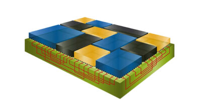
The slowing of Moore’s law has become a major driver to the chiplets way of implementing SoCs. Chiplets are small ICs specifically designed and optimized for operation within a package in conjunction with other chiplets and full-sized ICs. More companies are turning to 3D stacking of ICs and chiplets implemented in different process nodes optimal for the respective chiplets function. Designers can also combine 3D memory stacks, such as high bandwidth memory, on a silicon interposer within the same package.
Delivering 3D IC innovations faster
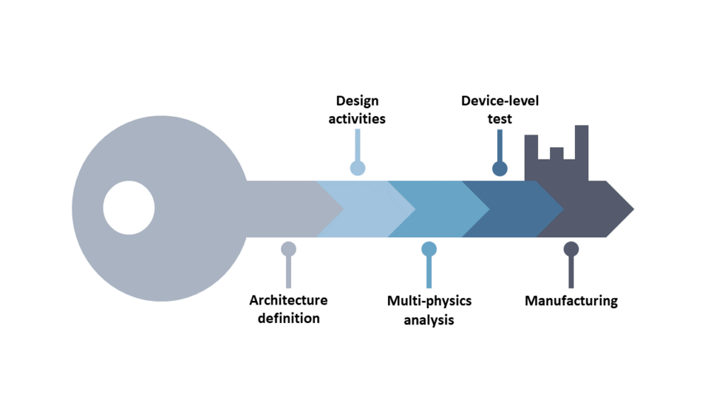
When new 3D IC capabilities are ready for mainstream, their mass adoption success depends on how easily, quickly, effectively and efficiently a solution can be delivered. While the 3D IC manufacturing technology may have become mainstream, there are some foundational enablers for a successful heterogeneous 3D IC implementation. The following must be considered and addressed early in the design process:
- System Co-Optimization (STCO) approach
- Transition from design-based to systems-based optimization
- Expanding the supply chain and tool ecosystem
- Balancing design resources across multiple domains
- Tighter integration of the various teams
Affordable and comprehensive design for test (DFT) of 3D stacking die devices
Developers of high-end semiconductor products that face manufacturing limitations with respect to die sizes are investing in 3D stacked die technology. These advanced designs already push current DFT solutions to the limits: tool run time, on-chip area, test pattern count, and test time. How then, can designers manage DFT for 3D stacked die devices?
Five key workflows for 3D IC packaging success
Five workflow adoption focus areas provide immediate heterogeneous integration capability benefits while establishing a managed methodology adoption and migration process that minimizes disruption, risk, and cost. These focus areas bring heterogeneous integration-based chiplet design within reach of mainstream manufacturers.
The 5 key workflows for 3D IC packaging
With the UCI-Express standard is driving the adoption of heterogeneous chiplets integration and with it the adoption of 3D IC implementations. When a new capability gets ready for mainstream, its mass adoption success depends on several things. While the foundational enablers are important, they are not sufficient for easily, quickly, effectively, and efficiently delivering a successful solution. Standardized protocols are needed to offer plug-and-play compatibility between chiplet suppliers.
With new requirements and signoffs, design tools evolve to meet and resolve any new challenges that arise. What the mainstream users need is a way to best use the tools to get an edge in the competitive marketplace. Chiplet based designs add levels of complexity that must be understood and planned for in each of these areas.
- Workflow Adoption
- Early Planning and Predictive Analysis
- Automating Interface-Based Design
- Thermal, Stress and Reliability Management
- Test and Testability
- Driving Verification and Signoff
To answer the questions raised and learn more about topics and solutions outlined in this blog – download this comprehensive ebook where we provide valuable insights, discussion, resources and describe the workflows that will help you achieve 3D IC packaging success.
Click here to learn how you can deliver product differentiation faster using 3D heterogeneous integration of node and performance-optimized chiplets with Siemens EDA’s market-leading 3D IC technology solution.