Understanding 3D IC Technology: Unveiling the Future of Integrated Circuits
In the fast-evolving landscape of integrated circuit (IC) technology, 3D ICs have emerged as a groundbreaking innovation that promises enhanced performance, reduced power consumption and compact designs. As technological advancement leaders in the field, we delve into the intricacies of 3D IC technology, elucidating its significance, architecture, benefits and applications.
What is 3D IC technology?
Over the past 40 years, the semiconductor industry has witnessed significant advancements in application-specific integrated circuit (ASIC) technology nodes, resulting in improved performance. However, as we approach the limitations of Moore’s law, the process of scaling devices becomes increasingly difficult. Shrinking devices now takes more time, is more expensive and poses challenges in terms of technology, design, analysis and manufacturing of these chips. Thus, enters 3D IC.
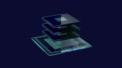
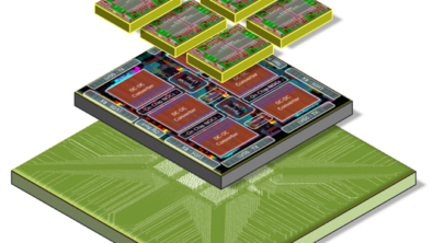
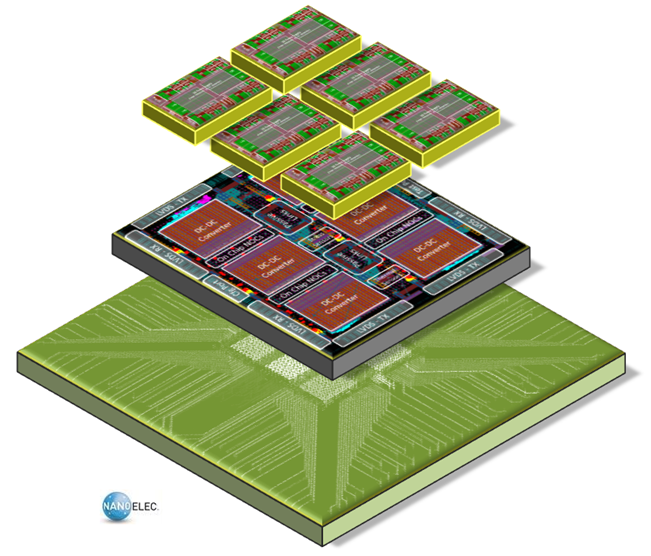
A chiplet is an Integrated Circuit (IC) that has been designed and optimized to be integrated with other chiplets in a single package. These chiplets may be integrated and assembled on a silicon or organic interposer which is referred to as 2D or 2.5D or vertically assembled which is referred to as 3D. The term 3D IC refers to an electronic component comprised of 2 or more chiplets integrated into a single package using 2D and/or 3D assembly advanced packaging technologies. Design teams break down traditional monolithic architectures into smaller functional chips or chiplets, which are then integrated into a single package. By utilizing this approach, 3D IC integrated circuits occupy less physical space while achieving significantly enhanced performance compared to traditional monolithic technologies.
As consumer electronic devices continue to become more technologically advanced and interconnected, designers need to explore new methodologies like 3D ICs to overcome the limitations of traditional approaches. The complexity of these devices is increasing with more features and intricate electronic circuit designs, which in turn require more processing power. To meet these growing demands, designers must adopt new techniques for designing and connecting chips.
To learn more about what 3D IC technology is and how it is evolving, read The Beginner’s guide to 3D IC
The architecture of 3D ICs
As stated, 3D IC is often referred to as a path to “more than Moore;”. This is a reference to Gordon Moore’s observation that the number of transistors on a semiconductor doubles every two years and along with that, the associated speed, capacity and throughput. Heterogeneous semiconductor integration is an inflection point that’s not only bringing new architectures into the market but also disrupting the engineering process. Low latency, high-bandwidth data movement 3D IC enables
companies to partition a design and integrate silicon IP at the most appropriate process node and process, providing lower manufacturing costs, higher wafer yields, lower power consumption and overall lower costs. View this infographic to learn how to Unlock the potential of 3D IC.
3D IC architecture has led to design teams turning to the disaggregation of once monolithic implementation architectures into several smaller functional chips or chiplets which are then reaggregated or integrated using a high-performance 3D IC package. This innovative approach allows different functional layers, such as logic, memory, and sensors, to be interconnected, paving the way for increased communication density and reduced interconnect lengths. The “through-silicon via” (TSV) technology plays a pivotal role in connecting these layers in 2D/2.5D designs, facilitating the seamless flow of data between them. Hybrid bonding technology are used to facilitate the interconnect between stacked chiplet 3D designs.
Read this ebook titled “Launching The Full Potential Of 3D IC With Front-End Architectural Planning” to learn more about 3D IC front-end design planning and predictive analysis.
Benefits of 3D IC technology
The adoption of 3D IC technology ushers in a multitude of benefits that elevate the performance and efficiency of electronic devices. Notable advantages include:
Enhanced Performance: The reduced interconnect lengths and increased communication density within 3D ICs result in faster data transfer rates and lower latency. This translates to improved overall device performance.
Lower Power Consumption: The shortened interconnects within 3D ICs mitigate signal degradation and energy loss, leading to reduced power consumption compared to their 2D counterparts.
Compact Designs: 3D ICs enable the integration of multiple functionalities in a smaller footprint, making them ideal for devices where space is a premium.
Thermal Management: The vertical arrangement of components in 3D ICs facilitates efficient heat dissipation, addressing thermal challenges associated with densely packed electronics.
Applications of 3D IC technology
3D IC technology is versatile and opens doors to a wide range of applications across various industries.
The emergence of 5G technology is enabling a wide range of applications in mobile, IoT, automotive and other sectors. Consequently, there is a need for various design processes to cater to these diverse applications. Currently, the monolithic design process focuses on process technology and system architecture to accommodate increased functionality. However, there is significant potential in 3D IC designs to enhance small-sized devices by providing improved interconnects, higher performance and lower power consumption. The benefits of 3D ICs span many industries and include less power, higher performance, smaller sizes, more memory and increased bandwidth.
For example: The rapid growth in bandwidth requirements between a smartphone’s processor and memory, particularly when it comes to tasks like video streaming, presents a significant challenge to the conventional interconnect systems used to connect packaged chips. Power consumption and management are concerns, and to address them you need to minimize the length of a system’s major bus lines by tightly packaging components together. This is an ideal application for 3D IC.

Some notable 3D IC applications include:
High-Performance Computing: In supercomputers and data centers, 3D ICs empower complex computations and data analysis by providing exceptional processing power and reduced latency.
Consumer Electronics: Mobile devices, wearables and smart appliances benefit from 3D ICs’ compact designs, enhancing user experience and extending battery life.
Automotive Industry: Advanced driver-assistance systems (ADAS) and autonomous vehicles rely on 3D ICs to process vast amounts of sensor data in real-time, enabling safer and more efficient transportation.
Medical Devices: Medical imaging, diagnostic tools and implantable devices leverage 3D ICs’ performance capabilities to provide accurate and rapid results.
Learn about the 3D IC design workflows available to designers in this eBook entitled: Semiconductor packaging: making the right connections in 3D IC design
The future of 3D IC technology
As technology continues its rapid evolution, the future of 3D ICs shines brightly. Researchers and engineers are tirelessly working to enhance packaging technologies, optimize manufacturing processes, and explore novel materials to further unlock the potential of 3D ICs. The integration of artificial intelligence and machine learning into 3D IC design holds the promise of even more efficient and intelligent electronic devices.
Siemens advantages:
- Enable digital transformation through co-design, co-simulation and automated checking
- Most comprehensive coverage for performance validation and design verification available
- Better resource utilization with concurrency, physical IP block reuse and platform flexibility
- Industry-leading capacity, performance and manufacturing execution.
To learn more about the future of 3D IC, listen to The future of semiconductor design podcast, in which industry experts discuss 3D IC concepts and the latest trends: chiplet designs, IC packaging, multi-die verification, golden netlists, electrical signoff, system analysis, and more!
In conclusion, 3D IC technology has transcended the boundaries of conventional integrated circuitry, ushering in a new era of performance, efficiency and compactness. Its innovative architecture and myriad benefits make it a cornerstone of modern electronics, with applications spanning across industries. Embracing 3D IC technology paves the way for a future where electronics are not only more powerful but also more intelligently designed.
Now it’s your turn to engineer a smarter future faster!
Discover how Siemens’ heterogenous 3D IC solution helps you create designs that meet or exceed your PPA goals and improve the differentiation, profitability and time-to-market of your next market-leading product. Visit the 3D IC design solutions web page and discover how Siemens’ heterogeneous package workflow catapults you into the future of IC design today!