Package designers need assembly-level LVS for HDAP verification
While advanced integrated circuit (IC) packaging is a fast-growing market, comprehensive package verification still has a ways to go. Unique package connectivity issues, such as missing or misplaced interposer/package bumps/pads, pin naming and text labeling issues, and the like, require new and enhanced LVS-like verification techniques that can move across the entire package to ensure proper connectivity and performance. With its native support for packaging file formats, automated analysis of high density advanced packaging (HDAP) connectivity verification requirements, and integrated assembly-level design rule checks (DRC) and layout vs. schematic (LVS) checking, the Calibre 3DSTACK tool provides a significant advantage over traditional SoC LVS flows.
Contrary to what you might think, advanced IC packaging is real. Several leading foundries and outsourced assembly and test (OSAT) companies already offer HDAP services to their customers.
The two most common approaches are 2.5D-IC and fan-out wafer-level packaging (FO-WLP). See Figure 1. In 2.5D-IC, the design is owned by the IC design group and requires an IC-oriented design approach. In FO-WLP, design approaches based on spreadsheets are used. Historically, automated LVS signoff has not been popular in packaging, but as HDAP evolves, the need for an automated LVS-like flow has become apparent.
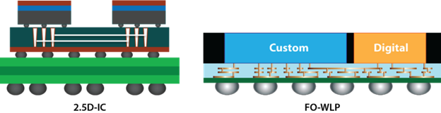
Figure 1. 2.5D -IC and FO-WLP
The manufacturing processes and ownership may vary for different package technologies. However, the verification process remains mostly the same, despite using different file formats and tools. An automated package flow, similar to LVS, needs to ensure proper connections of the interposer/package GDSII between die-to-die and die-to-C4/BGA bumps. EDA tool suppliers are developing new verification solutions to cater to the needs of the HDAP market.
This white paper provides insights and answers to some common questions that designers can use to help simplify and speed up debugging like:
- Do I have pin naming issues in the source netlist vs. the layout?
- Do I have GDSII export issues?
- Do I have text labels issues?
- Do I have port mismatch issues?
What about power/ground connectivity checking?
In traditional LVS flows from the system-on-chip (SoC) world, a design will pass LVS if there is one valid connection for VDD (or VSS), even if there is a broken VDD (or VSS) connection somewhere else. This happens because of the way SoC LVS engines extract the layout netlist. This white paper also provides solutions to detect power/ground issues that are often assumed detected downstream.
Download this whitepaper written by Tarek Ramadan, 3D IC Technical Team Leader, Siemens EDA who describes why IC package designers need assembly-level LVS for HDAP verification.
CLICK HERE to learn how you can deliver product differentiation faster using 3D heterogeneous integration of node and performance-optimized chiplets with Siemens EDA’s market-leading 3D IC technology solution.