System-level, post-layout electrical analysis for high-density advanced packaging (HDAP)

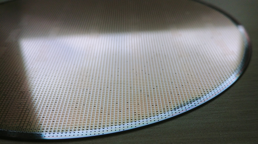
High-density advanced packaging (HDAP) continues to be the promising “More” in the “More than Moore” approach for improved form factor, functionality, and integration of multiple dies built using different technology nodes. As HDAP designs like fan-out wafer-level packaging (FOWLP) become more popular, the need for post-layout simulation (analog) and post-layout STA (digital) flows to augment basic physical verification (DRC and LVS) is growing.
HDAP offerings from outsourced assembly and test (OSAT) companies and foundries are continuously increasing. However, the full commercial productization of such offerings will require the assurance of both an acceptable yield and correct (as intended) functionality. This assurance will come from the availability of proven and qualified electronic design automation (EDA) tools and flows that can be used by the design houses to build HDAPs with the confidence that they are compliant with the foundry/OSAT requirements and recommendations.
As HDAP technologies and flows mature, system-level designers want to know:
Q: “Is package design rule checking (DRC), assembly-level LVS, and layout vs. layout (LVL) verification (die-to-package alignment, scaling, orientation, etc.) sufficient to guarantee the functionality and manufacturing of the HDAP are correct?”
A: The answer is generally no (for now) as it is dependent on just how complicated the HDAP is.
As HDAP technologies continue to resemble IC technologies, it is evident that while the physical verification processes for HDAP are making strides, they are merely a fraction of a larger, more extensive process. This comprehensive flow must address a thorough system-level electrical analysis. Naturally, this necessitates enhanced support from EDA tools to guarantee efficient, precise, and automated flows that enable package designers to meet their market deadlines and fulfill expectations.
HDAP post-layout electrical analysis
For a digital-based flow, the designer must run static timing analysis (STA) on the complete HDAP system, including parasitics, to ensure it meets the overall system timing budget. From an EDA perspective, building an automated flow to support these checks/analyses assures that these processes can occur in a consistent, repeatable manner while ensuring accuracy and minimizing runtime.
In general, EDA approaches take one of two paths.
- Single Cockpit or
- Tool-agnostic

System-level post-layout analysis
To conduct post-layout circuit simulation (analog/RF) or STA (digital) for an HDAP, a system-level layout netlist that accounts for the overall system parasitics must be generated. Before this, not only does the HDAP need to be verified for connectivity (LVS-clean). The layout netlist must include several components, as described below.
- System-level connectivity
- Die-level layout parasitics
- Package-level layout parasitics
- Die/package interface parasitics
What about pre-processing?
To ensure accuracy in the results, this flow must consider two questions about the HDAP design before generating the interface RC model and running the parasitic extraction process.
- Is interface extraction required?
- Which layers from each die must be included in the interface?
As HDAP approaches become more popular, the need for post-layout simulation and post-layout STA flows to augment basic physical verification (DRC and LVS) is apparent. By providing an accurate, automated flow that generates the required HDAP netlist for simulation/STA, EDA companies enable HDAP designers to ensure that the HDAP will perform as designed.
So, what does the EDA flow for HDAP post-layout static timing analysis look like? That is, one that generates HDAP system-level connectivity while accounting for die, package, and die/package interface parasitics and ensures confidence in HDAP manufacturability and performance?
This whitepaper written by Tarek Ramadan, 3D IC Technical Team Leader at Siemens EDA entitled “System-level, post-layout electrical analysis for high-density advanced packaging” addresses the questions posed in this blog as well as provides insights and defines automated flows that enable package designers to meet their market deadlines and fulfill expectations.
CLICK HERE to learn how you can deliver product differentiation faster using 3D heterogeneous integration of node and performance-optimized chiplets with Siemens EDA’s market-leading 3D IC technology solution.


