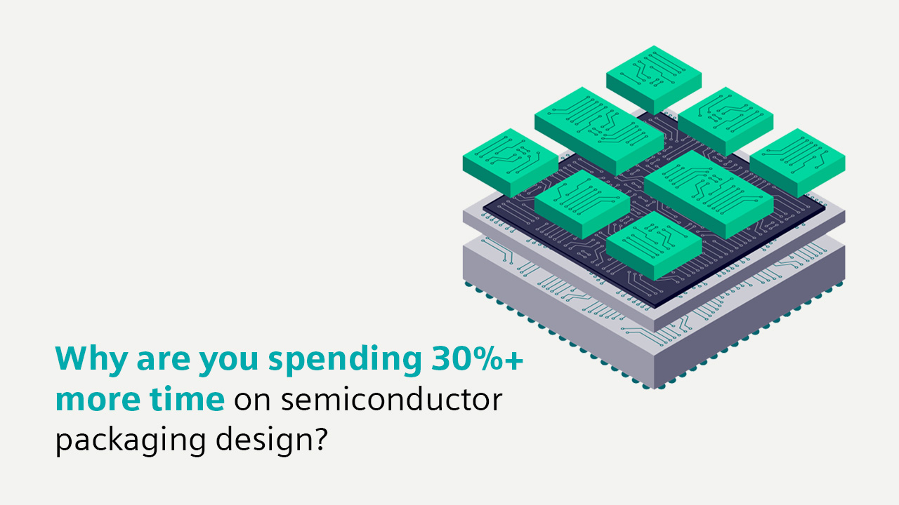
Why are you spending 30%+ more time on semiconductor packaging design?
Designs are just getting bigger and more complex
Yes, an obvious aspect is increasing design complexity. Packages are now a heterogeneous integration platform and no longer just a connector between the chip and the printed circuit board. As an HI platform their goal is to integrate, connect and optimize multiple die together, these could include ASIC logic or chiplets, memory, voltage regulators and discrete’s. Your first problem could be your existing legacy design tools, tools that were developed for single die organic laminate BGA designs.
Complex designs come with complex metal planes
Many of todays advanced package substrates require complex filled metal plane areas to deliver the power to the die and these metal-filled plane areas are required to pass the exacting fabrication requirements of the substrate supplier and/or OSAT. Last generation’s package design tools really struggle with complex filled metal areas, especially those where strict multi-aperture outgassing and area metal balancing rules. These legacy tools often apply workarounds such as “fast” mode to get over their performance issues. Of course, these “fast” modes are typically not manufacturing ready/correct and usually have to undergo a post process phase or “smooth” mode which takes time, sometimes considerable time, extending the design cycle.
High Bandwidth Memory (HBM)
Now if you’re doing high performance computing (HPC) related package design, and that includes datacenter devices, AI processors, network processors, VR etc. then HBM is likely to be a new challenge you’ll face. HBM has exacting routing rules and is a massively parallelized interface typically implemented as four 4-Hi stacks with a total memory bus width of 4096 bits. Routing such a wide bus and getting it within specification can take a long time unless your design tool is capable of intelligent channel replication, including the ability to update replicated channels due to post route edits.
Reusing known good design IP
Another area that can easily increase design time is the lack of support for common physical design IP reuse. Advanced packaging often has repeated structures, complex via arrays is one such example, and without an efficient way to define and reuse them, such as a library element, you’re left with hours of manual creation and editing, not just on your design but across other designs as well.
Deploying team design to shrink design cycles
Now with advanced packages containing multiple heterogeneously integrated die/chiplets over device size and complexity naturally requires a lot of designer effort and expertise, which increases the design cycle time. One way to attack this is by deploying multiple designers concurrently to the same design often known as team design. The latest generation of semiconductor package design tools come with built-in dynamic team design where each designer can see in real-time what the other designers are creating/editing and provide soft fences to prevent one designer from overriding another designer’s work.
As you can see there can be many reasons as to why your design cycles are increasing, and this blog is just a subset of what you may be facing on your next design. But do not despair, there is a way out of the tunnel and that’s where Siemens can help. To learn more about how Xpedition Package Designer (xPD) can help download our eBook: The six key differentiators of Xpedition Package Designer (xPD).