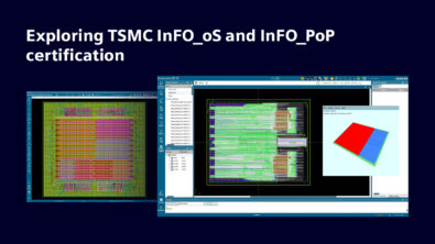
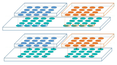
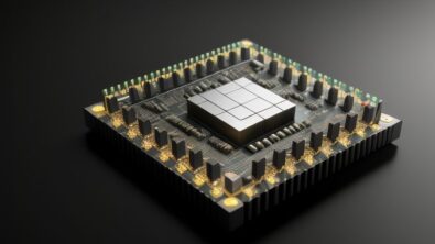
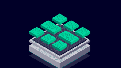
Monolithic scaling limitations drive the growth of 2.5/3D multi-chiplet, heterogeneous integration that enables PPA targets to be met. Our integrated flow addresses prototyping challenges to signoff for FOWLP, 2.5/3D IC, and other emerging integration technologies.

Learn more about semiconductor packaging design and verification.

Featured posts

Latest posts

System-level, post-layout electrical analysis for high-density advanced packaging (HDAP)

HDAP designs like FOWLP need post-layout simulation (analog) and post-layout STA (digital) flows to augment basic physical verification DRC and LVS.

Crossing the chasm: Bringing SoC and package verification together

3D IC package designers need assembly-level LVS for HDAP verification.

Package designers need assembly-level LVS for HDAP verification

While advanced integrated circuit (IC) packaging is a fast-growing market, comprehensive package verification still has a ways to go. Unique…

An image of an IC package design in Xpedition Package Designer with text that says: Achieving substrate supplier fabrication requirements: a designer's guide

Achieving substrate supplier fabrication requirements: a designer’s guide

Designing advanced package layouts with large areas of metal can be a daunting task, given the stringent requirements imposed by…

Understanding 3D IC Technology: Unveiling the Future of Integrated Circuits

Delve into the world of 3D IC technology, its architecture, benefits, and applications. Learn how it’s reshaping the future of integrated circuits for enhanced performance and efficiency.

Image of chiplets with text onscreen saying HBM

High Bandwidth Memory (HBM): Unleashing the power of next-gen memory technology

In the ever-evolving realm of semiconductor technology, one innovation stands out above the rest: High Bandwidth Memory (HBM). Offering unparalleled…

What's new in Xpedition IC Packaging

What’s new in Xpedition IC Packaging VX.2.14

The new VX.2.14 release of Xpedition IC Packaging includes improvements and enhancements to both Xpedition Substrate Integrator and Xpedition Package…

SemiWiki Podcast – An expert panel discussion on the move to chiplets

Listen in as Tony Mastroianni Advanced Packaging Solutions Director – Siemens EDA along with Saif Alam Vice President of Engineering…

system technology co-optimization

Shifting left with system technology co-optimization for IC packaging

We have witnessed and learned about the industry’s significant shift in semiconductors. The traditional approach of transistor scaling, once universally…