Interconnect Robustness Depends on Scaling for Reliability Analysis
By Matthew Hogan, Mentor Graphics
Fast simulation and PEX are both crucial to interconnect robustness verification. Can your tools scale up to the task?

The safety net of design margins that were once available to designers has disappeared. Whether you’re implementing a new design start at your “next” node or an established node, the desire for greater functionality has eroded what margins used to exist. This tightening of design margins is further exacerbated by an increasing industry-wide focus on reliability, driven by both consumer demand and an expanding array of standards for performance-critical electronics. This focus seems to be landing equally on both devices and interconnect. Gone are the days when (rough) hand calculations or visual inspection of designs were sufficient to provide the level of confidence needed to proceed against time-sensitive tapeout schedules and tight time-to-market windows.
Now present in both digital and analog designs is the need to validate interconnect robustness, or resistance to failure. The old technique of “counting squares,” where each “square” of a specific size was given a resistance value for each metal layer, and other manual methods seldom provide the necessary accuracy.
For a design to be “LVS clean,” all that’s required is a single connection. Not a great way forward if you are expecting to shunt any reasonable current through those connections. The same is true for blocks connecting to wide power busses, with slender metallization. Figure 1 shows several examples of LVS-clean layouts with very low robustness, and how they could be improved.
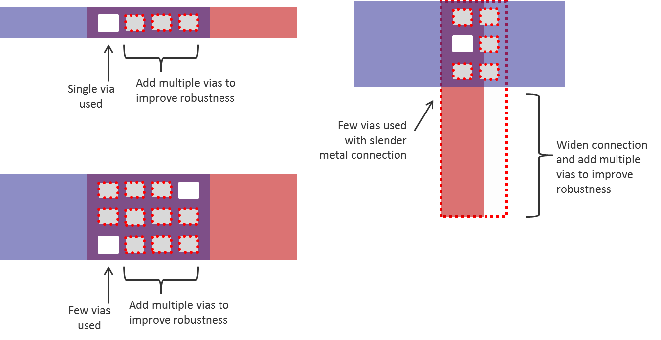
Figure 1. Inadequate via and interconnect connections within layers.
Parallel paths and unexpected layer transitions make point-to-point resistance (P2P) simulations an invaluable tool for validating that low resistance paths between design elements exist. Current density (CD) simulations provide more detail, and not only allow designers to consider the suitability of the metal width, but also provide an opportunity for detailed analysis of layer transitions.
Early interconnect evaluation
Validation of individual intellectual property (IP) blocks before final integration into the system-on-chip (SoC) provides an early look at possible robustness issues. Far too often, design teams feel the need to wait until final chip assembly to validate full path interconnects. While this is an important task that must be completed, validating each of the IP blocks early in the design process, when changes can more easily be made, provides important feedback on what to expect in the final design. In addition to focusing on each IP block, designers must also consider functional assemblies, even before they actually exist. Where will the electrostatic discharge (ESD) protection blocks be integrated? How will the lower levels of IP be validated for interoperability? These are all important design flow considerations.
At smaller process nodes, particularly those using FinFETs, ESD circuits require a larger number of (often interdigitated) devices to provide adequate protection. The ESD target levels that you design to can greatly impact the area and number of these devices. Verification of these structures, particularly the interconnect to clusters of these devices, is of critical importance. Validation at the lowest design level possible, as early in the design process as possible, enables efficient design flows for each technology node. Depending on the design style and its robustness/reliability requirements, it may be necessary to critically look at detailed combinations of input/output (IO) pads to power clamp devices. This type of analysis may require a significant number of individual simulations to capture all combinations of IO1 through each of the power clamps (Figure 2).
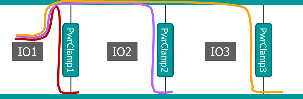
Figure 2. Multiple simulations are needed to capture all combinations of IO1 through each of the 3 power clamps.
Full chip evaluation
In addition to this focused analysis at the IP level, understanding the context of IP use in the full-chip SoC is also an important consideration. As with validating the IP-level interconnect, full-chip evaluation requires a strategy that matches your workflow. Do you only need to validate interconnect to the ports of your IP, or must you go all the way to the device level?
As is standard in LVS full-chip runs, designers performing interconnect robustness analysis may exercise their verification tools for P2P and CD simulations at the device level. Leaving nothing to chance, this evaluation looks at the entire full-chip path, often looking at different combinations of ESD protection paths. If you use a comprehensive verification toolset, the good news for all these simulation paths is that you can parasitically extract all of the pin-pairs that need to be evaluated at the same time. The combinations that must be simulated can re-use these parasitics to perform the next simulation (Figure 3). This re-use is critical for minimizing turnaround time (TAT) while scaling to the number of simulations required for detailed analysis.
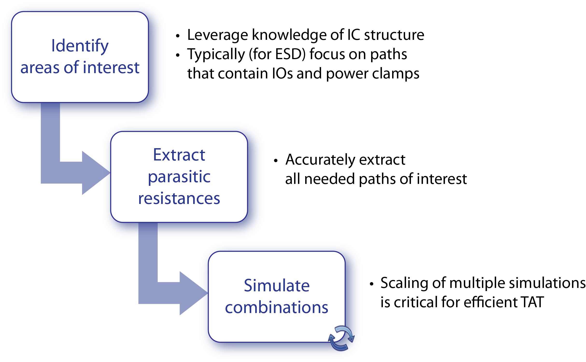
Figure 3. Scaled simulations are essential to minimizing TAT while ensuring accurate and complete analysis.
Conclusion
The need to validate interconnect robustness is now a given at advanced nodes. However, accepting simulation runtimes that take days, or even weeks should be a thing of the past. With interconnect robustness a critical aspect of reliability, fast simulation and parasitic extraction is essential for both schedule and market success. Early analysis within the design flow helps alleviate last-minute discovery of critical errors, providing the opportunity for fixing without significant adverse impacts to product schedules. Detailed analysis of interconnect, particularly for P2P and CD in ESD environments, with a reliability verification tool capable of quickly performing complex simulations, provides both accuracy and the necessary coverage in an acceptable timeframe. The early discovery of interconnect robustness issues, combined with the ability of your verification tools to easily and efficiently scale from IPs to SoCs, can ensure timely design completion while enhancing design reliability, a combination that can provide a new safety net—for your bottom line.

This article was originally published on www.semimd.com