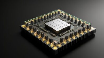
Workflows for tackling heterogeneous integration of chiplets for 2.5D/3D semiconductor packaging.
The demand for increased power and performance in semiconductor packages has surged. As more die and chiplets are integrated into…
Advanced nodes and 3D-IC packages require new and enhanced parasitic extraction processes that can resolve a variety of complex parasitic issues in these designs.
HDAP designs like FOWLP need post-layout simulation (analog) and post-layout STA (digital) flows to augment basic physical verification DRC and LVS.
3D IC package designers need assembly-level LVS for HDAP verification.
While advanced integrated circuit (IC) packaging is a fast-growing market, comprehensive package verification still has a ways to go. Unique…
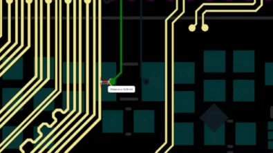
Designing advanced package layouts with large areas of metal can be a daunting task, given the stringent requirements imposed by…
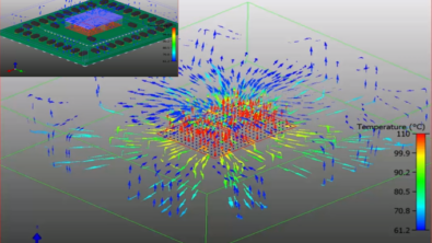
In the ever-evolving realm of semiconductor technology, one innovation stands out above the rest: High Bandwidth Memory (HBM). Offering unparalleled…
We have witnessed and learned about the industry’s significant shift in semiconductors. The traditional approach of transistor scaling, once universally…