How to get your system-in-packages right
People have been designing “modules” or system-in-packages (SiP) for a number of years; but in the last 3-5 years, I have seen a rapid increase in complexity, brought about by the need to further miniaturize electronics.
Automotive ADAS and autonomous driving is one great example of this. As vehicles need more electronics and compute power to analyze sensor data and make decisions, the need to find ways of packaging these new electronics increases. Additionally, many companies are looking at retargeting systems that were once achieved via a PCB, but now re-implementing as a SiP or module.
Utilization of system-in-packages in semiconductor packaging
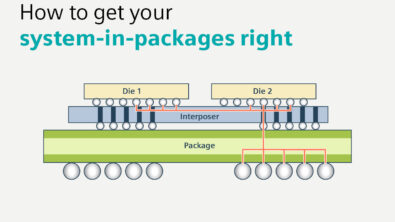
System-in-package or modules, are designs with multiple high-yield bare die semiconductors integrated together within a single package to form a system or sub-system. This approach enables higher densities, greater device functionality, and improved overall silicon yield. Not only are they growing in importance and usage, but these designs also continue to grow in complexity and density due to advanced process nodes and shrinking substrate feature size support. So it’s now vital that they are validated as an assembly to ensure correctness before they hit manufacturing.
DRC/LVS verification – a new design verification approach
Traditionally, the industry has used layout versus schematic (LVS) to perform a complete electrical verification of module and system-level designs. Meanwhile, design rule checking (DRC) performs verification of the physical design to ensure all metal layers meet fabrication rules. What’s new is the combination of DRC and LVS to perform three-dimensional assembly verification. With this approach, you can look for and identify a variety of critical issues, if they exist in a design, such as unintentional shorts or opens, misalignment between die bumps and pads on the substrate, the shrinkage factor applied to a die but not properly accounted for on the package substrate, a last-minute change to the die not communicated to the package designer, and more. By performing DRC/LVS verification prior to tape-out of the SiP or module, design engineers can be confident that the intended logical and physical connectivity matches the true tape-out design data.
Now logical verification ensures that the physical connectivity of a design matches the design netlist. This means identifying all shorts, opens, floating pins, or isolated metals to ensure proper connectivity throughout a design. A DRC/LVS verification solution must be able to perform automated logical verification by comparing connectivity of physical geometries, often in the format of GDSII, against the intended logical netlist. Logical verification should not only be completed within each substrate, but also across substrates, to provide confidence in the accuracy of the entire system. Real-die GDS data should be used during DRC/LVS verification to ensure connectivity of the package matches the tape-out die GDS data.
This entire process can be reviewed in more detail by downloading this technical paper written by one of our technical solutions sales application engineers who describes the use model of one of the world’s largest fabless semiconductor companies.