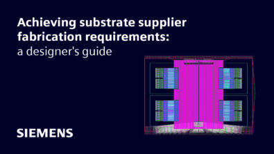
Achieving substrate supplier fabrication requirements: a designer’s guide
Designing advanced package layouts with large areas of metal can be a daunting task, given the stringent requirements imposed by substrate fabricators. The challenges arise from the need to ensure the structural integrity of the substrate while minimizing the risks of issues like delamination and warpage. To tackle these challenges, designers must navigate a maze of rules, design criteria, and diverse substrate technologies. In this blog post, we’ll explore the importance of meeting substrate fabricators’ requirements and discuss three common methodologies to achieve the desired results. Furthermore, we’ll focus on how Xpedition Package Designer’s automated capabilities can make this complex process more efficient.
The complex world of metal fill requirements
Substrate fabricators impose strict requirements on metal fill, primarily to address two critical concerns:
- Delamination Risk: In advanced packages, dielectric and metal layers are often incredibly thin, sometimes as thin as 15 µm or less. During the build-up and Redistribution Layer (RDL) process, delamination can occur due to trapped pockets of gas within the structure.
- Warpage: Uneven conductor densities on the same layer or across layer pairs can lead to warpage in the package or the wafer, impacting the structural integrity of the design.
To mitigate these issues, substrate fabricators discourage the use of solid metal planes or large metal areas. Instead, they provide designers with strict metal fill requirements, often in the form of rules, design rule checks, and design rule manuals (DRMs). Adhering to these requirements can be a challenge due to the combination of complex issues and the diversity of substrate technologies from various vendors. But there are three key methodologies that designers employ to control and mitigate these issues.
Methodology 1: hatched filled metal areas with layer offsets
One of the most common methods to meet substrate fabricator requirements is to use hatched filled metal areas with layer offsets. This approach involves creating a grid-like pattern of metal within the designated area, allowing for the controlled flow of gases and minimizing the risk of delamination. By introducing layer offsets, designers can further optimize the design, making it more resilient and efficient.
Methodology 2: insertion of outgassing void patterns
The insertion of outgassing void patterns is another technique used by designers. These void patterns are strategically placed within metal-filled areas to facilitate the release of trapped gases during the manufacturing process. This reduces the risk of delamination and ensures a more stable substrate.
Methodology 3: addition/insertion of dummy metal fill
Dummy metal fill, also known as “dummy metal structures,” involves adding extra metal structures in areas where high-density metal is not required. This helps to balance conductor densities across layers, reducing the potential for warpage. By inserting dummy metal fill, designers can fine-tune the design to meet the fabricator’s specifications.
Xpedition Package Designer: your automation ally
Xpedition Package Designer offers automated capabilities that simplify the implementation of these methodologies, ensuring a more efficient and effective design process. Designers can leverage the software to create hatched filled metal areas with layer offsets, insert outgassing void patterns, and add dummy metal fill without the need for manual, time-consuming adjustments.
Meeting substrate fabricators’ requirements for metal areas and planes in advanced package designs is a critical aspect of the design process. To address the challenges of delamination and warpage, designers have at their disposal three key methodologies: hatched filled metal areas with layer offsets, the insertion of outgassing void patterns, and the addition of dummy metal fill. With the assistance of Xpedition Package Designer’s automated capabilities, designers can navigate this complex landscape more efficiently, reducing the risk of extended design cycles or engineering change orders (ECOs) due to fabricator rejection.
Achieving substrate supplier fabrication requirements is an essential part of the design process, and understanding these methodologies and using the right tools can make the journey smoother and more successful for designers in the world of advanced package design.
Read more about this concept in our eBook: IC Package physical design best practices