Shifting left with system technology co-optimization for IC packaging
We have witnessed and learned about the industry’s significant shift in semiconductors. The traditional approach of transistor scaling, once universally applicable, is no longer economically viable. As a result, the industry is now embracing innovative packaging technologies to meet the demands of system scaling and achieve cost efficiencies. This has led to the system technology co-optimization (STCO) concept, where a SoC type system is disaggregated, or partitioned, into smaller modules (also known as chiplets) that can be asynchronously designed by dispersed teams and then combined into a larger, highly flexible system using chiplet-based heterogeneous integration into an advanced packaging platform.
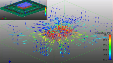
With this greater flexibility comes several additional challenges in the form of power integrity, signal integrity, thermal performance, warpage, and mechanical stress. Finding and having to fix such issues late in the design cycle becomes expensive. One solution is to take a shift-left approach where analysis is performed very early, and the results are used to drive design deci-sions as well as make corrections to mitigate the risk of verification failures later in the design flow.
So let me explain how such early analysis in complex advanced packaging flows can enable designers to spot potential issues early to avoid built-in constructs that cause design failures and require major redesign work. While detailed post layout verification analysis of a completed design can offer very accurate results, it is way too late in the process to provide value. The shift-left approach entails applying multi-physics analysis very early in the design process: at the prototyping and design planning stage where very little is known about the design. In this blog I will focus on power and signal integrity prototyping in STCO, but the approach can be applied equally to thermal, warp, and mechanical stress analysis.
The benefits of STCO
Now STCO brings many benefits but also new challenges. It enables teams to work in a concurrent yet asynchronous manner using dispersed design teams. Each design block can be worked on concurrently by different teams independently of each other. However, to do this, the data for all the blocks must come together at some point, and this point is in the package planning. This is when we reassemble the disaggregated SoC functional blocks (chiplets) and examine the packaging options.
The partitioning, or disaggregation, that was made will impact our ability to build a working package as well as package costs. It’s clearly important how that disaggregation is made, yet it’s made by teams that generally don’t have the downstream insight or means to consider the packaging impact of their decisions.
How to reintegrate design blocks
This is the main challenge we need to solve: How to reintegrate the design blocks into an early package prototype that has enough information to drive multi-physics analysis to help guide the partitioning. This includes evaluating the connectivity between design blocks. This analysis gives us critical information. By feeding that gained knowledge back to the silicon team, they possess invaluable information to help reconsider the partitioning (if needed).
Building the package prototype
We are typically looking to get a higher performing, lower power solution. Regardless of how we partition, there are always multiple partitioning and integration options: finding the right one is what STCO is all about. There is likely more than one good solution, so to find out which is best, we build a package prototype that we can use to analyze and weigh each partitioning option of interest. Now we start building the package prototype incrementally and refine it as more data becomes available and refined over time. At the package prototype level, we are first able to esti-mate power integrity and signal integrity, so the initial best effort partitioning needs to become a package prototype.
The package prototype is just what the name implies, a model of the intended package, not a detailed implementation. We know the size of the design’s functional blocks or chiplets. We know their signals, and through a SystemVerilog description of the system, we know how they connect to each other. We may —or may not— have physical die information through LEF/DEF at this stage, but if we have, we can use it for a more detailed prototype.
Preliminary analysis
We can now start by calculating the number of power and ground bumps we need for each module and build a preliminary bump map. This data is enough to take our package prototype into power integrity tools and do some very early, preliminary analysis that will tell us if it looks OK or if we have any areas of concern. We would also characterize the signal I/Os and run pre-liminary signal integrity analysis to see if various 3D stacking configurations can give us the results we are looking for and, more importantly, if it fails at this level then we adjust the floorplan which can be at the chiplet level or the substrate level and analyze again. Once you have a prototype that meets expectation you can then move into detailed implementation without the risk of significant ECO’s.