High Bandwidth Memory (HBM): Unleashing the power of next-gen memory technology
In the ever-evolving realm of semiconductor technology, one innovation stands out above the rest: High Bandwidth Memory (HBM). Offering unparalleled performance compared to traditional memory technologies like DDR (Double Data Rate) and SDRAM, HBM is revolutionizing the world of electronic hardware-based products.
The HBM revolution
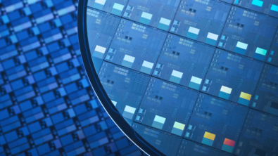
HBM is a game-changer in the memory technology landscape, providing a remarkable boost in both bandwidth and energy efficiency. This makes it a perfect fit for applications demanding rapid and efficient data processing. Whether it’s high-performance computing involving CPUs and GPUs, supercomputers, data center devices, or cutting-edge artificial intelligence implementations, HBM shines. The journey of HBM began in 2013 when SK Hynix introduced the world to its first HBM chip. Since then, it has evolved significantly, with the latest generation, HBM3, delivering a mind-boggling six times the data throughput compared to the original HBM.
HBM integration techniques
Today, integrating HBM into semiconductor designs typically involves the use of a silicon interposer. This interposer can take the form of a full interposer or utilize embedded or elevated bridge interposers like Intel’s EMIB. AMD’s Fiji GPU was the trailblazer, becoming the first device to utilize HBM, hitting the market in June 2015. However, it was Nvidia’s Hopper GH100, featuring HBM3, that stole the spotlight when it began shipping in March 2022.
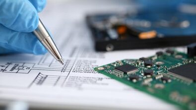
Despite its exceptional performance and data throughput capabilities, HBM does come with its set of challenges that cannot be overlooked. One of the most prominent challenges is the need for a costly silicon interposer, involving processes akin to those found in semiconductor foundries. Thermal management becomes paramount to ensure the final device operates as expected, given HBM’s sensitivity to high temperatures. Stable and efficient power delivery during switching operations is equally critical. Lastly, the manufacturing process and overall cost must be carefully considered.
Key considerations in HBM integration
When it comes to integrating HBM devices into a design, there are several key considerations that must be carefully managed:
- Signal integrity management and stable power delivery (this ensures optimal performance)
- Routing channels to accommodate the wide HBM buses
- Budgeting sufficient time for channel design and characterization
Revolutionizing semiconductor package design
The landscape of semiconductor package design is undergoing a seismic shift as companies embrace the integration of multiple chips and high-performance memory like HBM to push beyond the boundaries of Moore’s Law. The package, once merely a connector of dies to the PCB, has now evolved into a crucial platform in itself. This evolution necessitates a fresh design strategy and approach, often demanding new design tools.
With the advent of chiplet designs, the number of bumps on these devices has skyrocketed. Even an HBM module boasts nearly 2000 die-to-die connections. Regardless of the heterogeneous technology used in chiplet designs, design tools are indispensable. Traditional schematic designs no longer suffice for package designs; a netlist-driven format must be simplified to create a floor plan for a chiplet layout. Visual floor planning tools and design aids become essential to reduce cycle time and ensure repeatability during the design process.
Unlocking the potential of HBM
For those looking to delve even deeper into the world of HBM, our on-demand webinar offers invaluable insights. We address the complexities of HBM design, covering topics such as:
- Developing and optimizing a package floor planning process for four HBM stacks integrated with a logic SoC
- Explaining the creation of physical implementation designs and efficient HBM simulation
- Exploring the development of circuit replication blocks
- Discussing the critical aspects of Signoff and Tapeout
In conclusion, High Bandwidth Memory (HBM) has emerged as a powerhouse in the realm of memory technologies. Its exceptional performance and energy efficiency make it the go-to choice for a wide range of applications. However, HBM integration comes with its unique challenges, which demand meticulous planning and management. As semiconductor technology continues to evolve, understanding and mastering HBM design will be essential for staying at the forefront of innovation in the industry. So, join us on this journey as we unlock the full potential of HBM and explore the future of memory technology.