​3D IC technology trends: Microarchitecture in IC design

In this latest Siemens EDA 3D IC podcast episode, we explore microarchitecture’s crucial role in 3D IC design. Listen in…

​3D IC technology trends: how advanced IC packaging is changing the semiconductor industry

The semiconductor industry is rapidly evolving with 3D IC technology and advanced packaging solutions revolutionizing chip design and manufacturing. In…

Accelerate IC design innovation with Siemens: Navigating the future of 3D IC design to manufacturing

In the rapidly evolving semiconductor industry, the drive towards miniaturization and the integration of complex functions through advanced packaging and…

A deep dive into HDAP LVS/LVL verification

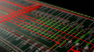
EDA companies are developing tools and workflows to support HDAP (High-density advanced packaging) LVS/LVL verification. Though the data for achieving “signoff-level” confidence is a work in progress, EDA companies are providing tools that can adapt to different levels of data availability and enable HDAP designers to execute HDAP LVS/LVL flows that are both productive and beneficial.

Parasitic extraction technologies: Advanced node and 3D-IC design

Advanced nodes and 3D-IC packages require new and enhanced parasitic extraction processes that can resolve a variety of complex parasitic issues in these designs.

System-level, post-layout electrical analysis for high-density advanced packaging (HDAP)

HDAP designs like FOWLP need post-layout simulation (analog) and post-layout STA (digital) flows to augment basic physical verification DRC and LVS.

3D heterogeneous integration devices with multiple 3D IC components

The impact of 3d heterogeneous integration on semiconductor device reliability

So far in our 3D IC blog series, we’ve discussed front-end design approaches to develop 3D IC-based devices, the importance…

Test engineer performing design rule checks manually for 3D IC heterogenous designs

Assembly level layout vs. schematic in 3D IC design verification

In our fifth podcast on 3D IC design workflows, we discussed what a 3D IC physical design workflow looks like,…

Engineer seated at computer studying physical prototype for early planning of interconnect systems and design verification workflows

Importance of early planning for interconnect verification in 3D IC physical design workflows

In our last podcast on 3D IC architecture workflows, we discussed how a system or microarchitectures determine how to partition…