IC package thermal resistance: Accurate modeling for system-level IC thermal reliability
As semiconductor devices grow more powerful and complex, effective thermal management has become a top priority in IC design. With increased transistor density and power consumption, even a small oversight in heat dissipation can result in performance degradation, reduced reliability, or catastrophic failure.
At the heart of this challenge lies a key parameter: IC package thermal resistance. Whether you are a chip designer, package designer, or thermal engineer, understanding, analyzing and debugging thermal effects is essential to ensure device reliability, especially as the industry shifts toward 3D ICs and heterogeneous integration.
In this in-depth guide, we explore the fundamentals of IC package thermal resistance, modeling strategies, influencing factors and how Siemens integrated 3D IC design and thermal analysis solutions including Calibre® 3DThermal, Innovator3D IC and Simcenter Flotherm help design teams address thermal challenges from early planning to system-level sign-off.
What is IC package thermal resistance?
IC package thermal resistance refers to the measure of a package’s ability to conduct heat away from the silicon die to its surrounding environment. Expressed in °C/W (degrees Celsius per watt), it indicates how efficiently heat generated at the junction is transferred through the package, board, and into the ambient environment.
Thermal resistance values are typically categorized as:
- θ<sub>JC</sub> (Junction-to-Case): Thermal resistance from the junction to a specified point outside of the package (case)
- θ<sub>JB</sub> (Junction-to-Board): Thermal resistance from the junction to the PCB
- θ<sub>JA</sub> (Junction-to-Ambient): Thermal resistance from the junction to the surrounding air
- ψ<sub>JT</sub> and ψ<sub>JB</sub>: JEDEC-defined parameters (rather than strict resistances) that help separate package-level and system-level thermal contributions.
These values help engineers model and manage thermal behavior throughout the IC’s operational lifecycle. Effective heat dissipation is critical for several reasons:
- Prevents overheating of the IC junction, maintaining device functionality
- Extends lifespan by avoiding accelerated aging and material degradation
- Protects signal integrity and timing performance
- Enables higher power density, allowing more functionality in a smaller footprint
- Supports thermal-aware test strategies in multi-die systems
Components of thermal resistance: A breakdown
Understanding the components of thermal resistance helps engineers select the right packaging technology and predict real-world thermal behavior:
| Resistance Type | Definition | Application |
| θ<sub>JC</sub> | Junction-to-Case | Useful for heatsink designs and thermal interface materials |
| θ<sub>JB</sub> | Junction-to-Board | Important for PCB-level thermal modeling |
| θ<sub>JA</sub> | Junction-to-Ambient | General thermal performance metric; influenced by airflow and system design |
| ψ<sub>JT</sub>, ψ<sub>JB</sub> | Junction-to-Top/Board | Derived metrics for more refined modeling under standardized test environments |
Each of these resistance paths contributes to the total heat dissipation capability of the IC package.
Factors that influence IC package thermal resistance
Several design and environmental parameters influence the thermal performance of an IC package:
- Die Size & Power Density
- Package Type (e.g., BGA, QFN, flip-chip)
- Substrate Material (e.g., BT resin, ceramic, organic laminates)
- Thermal Interface Materials (TIMs)
- Encapsulation & Lid Design
- Thermal Vias & Copper Pillars
- Heatsinking & Airflow Conditions
Choosing the optimal combination of these elements often requires trade-offs between thermal, electrical, and mechanical performance.
Learn about different IC Package Types in our comprehensive guide.
Strategies to reduce thermal resistance
Here are proven strategies to reduce IC package thermal resistance:
At the silicon level
- Add thermal TSVs (TTSVs) or keep high-power dies closer to the heat sink
- Use power gating/DVFS/clock gating to spread heat
- Simulate thermal effects with Calibre® 3DThermal in early design process
Package-level
- Use flip-chip bonding to lower die-to-package resistance
- Integrate thermal vias and heat spreaders into the substrate
- Select higher-k substrates
- Optimize bump/pillar density and footprint to improve vertical conduction
Board/system-level
- Apply heatsinks and thermal interface materials effectively
- Increase copper area in PCB for better conduction
- Use forced-air cooling or liquid cooling where applicable
distribution across all 3D components simultaneously throughout the simulation
duration.
Why die-level thermal analysis matters in 3D ICs
For traditional 2D monolithic chips, dies and packaging used to be designed in two separate development processes while thermal analysis was handled through simple, template-based modeling solutions. Any gross deficiencies can be flagged and fixed during post-layout simulation.
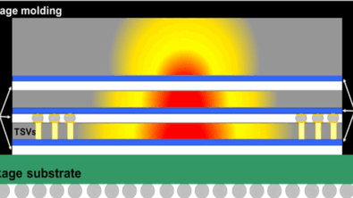
However, vertical stacking of active dies in 3D ICs has introduced new thermal challenges where active dies are brought into closer proximity. Limited thermal dissipation paths through complex material stacking create challenging thermal management scenarios such as:
- Die-die and die-package thermal hotspots
- Tight thermal coupling between tiers in 3D ICs
- Thinned dies and substrates
- Multiple through-silicon-vias (TSVs) and µ-bump arrays
- Nonuniform thermal conductivity in different directions
Interface thermal resistance, once mostly affecting package boundaries, has become a crucial factor within package structures.
Key thermal challenges in 3D IC packaging:
- Thermal bottlenecks between stacked dies
- TSV thermal resistance and stress
- Power-density-induced hot spots
- Die-to-die mechanical warpage due to thermal mismatch
For more on foundational and advanced packaging techniques, see:
3D IC Thermal Modeling and Simulation Best practices
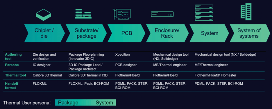
- Implement an integrated, thermal-aware design process: Thermal resistance must be evaluated in the context of the full design stack, including die, package, board, and system levels.
- Shift left thermal analysis: Integrate thermal considerations into system technology co-optimization (STCO) to avoid costly re-spins. Package and chip design engineers need to be able to quickly assess potential temperature-limiting factors in the early design stage.
- Use a unified 3D digital twin: Keep a consistent digital representation of every physical element in the design (a single source of truth). This ensures that thermal models accurately reflect the actual physical structure being developed.
- Automate model creation: Automated tools can reduce errors in handling sophisticated package geometries and material properties while making it easier for non-thermal experts to perform high fidelity analysis.
Integrated thermal analysis and 3D IC design process
Fixing thermal problems early is critical to 3D IC’s reliability and performance. Siemens EDA provides a comprehensive ecosystem of tools for package and chip design teams to identify hotspots early, making informed tradeoffs from architecture through signoff.
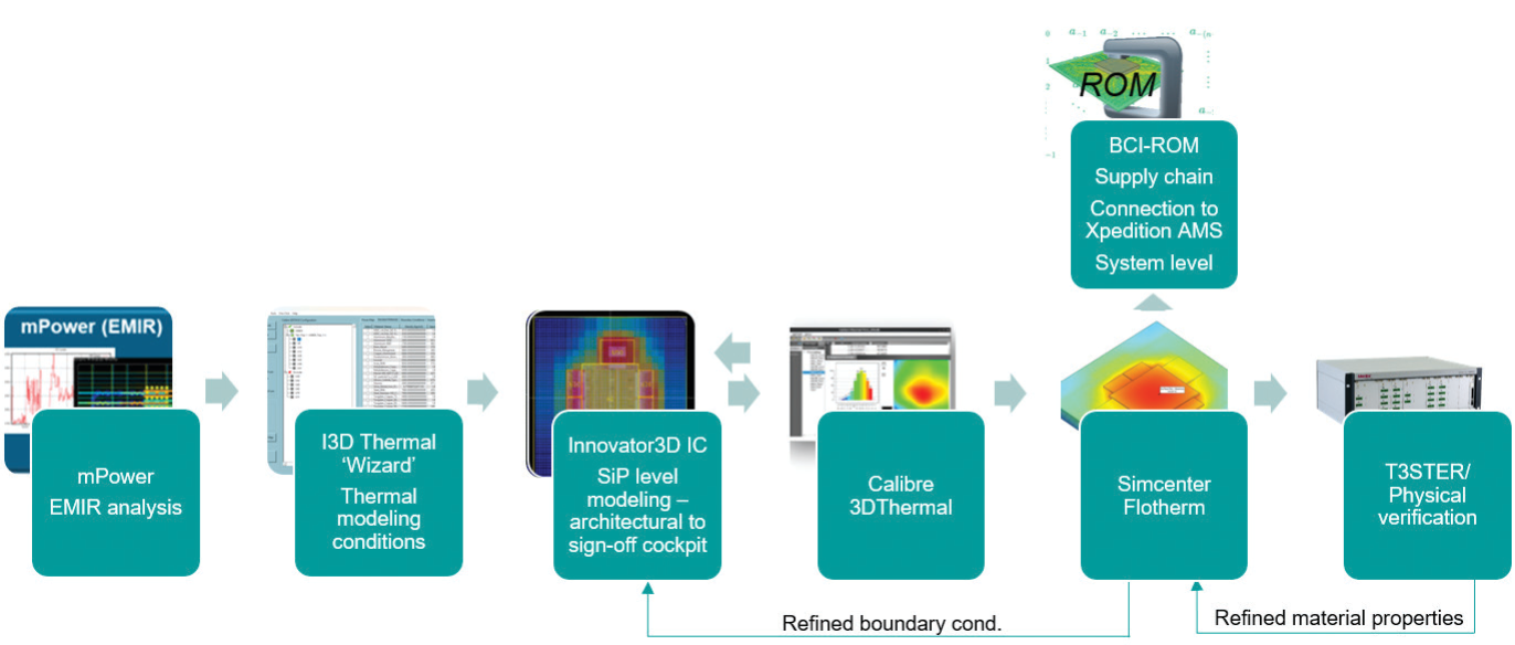
- Calibre® 3DThermal: End-to-end chip- and package-in thermal simulation, enabling thermal feasibility analysis, debug, and verification from concept to final design signoff.
- Simcenter™ Flotherm™ : Package-to-system thermal simulation to guide thermal management decisions from early architecture through verification.
- mPower: Analog and digital power integrity analysis from the smallest blocks to the largest full-chip layouts to verify power goals and performance.
- Innovator3D IC: A unified platform for chiplet, interposer and package design planning and simulation.
- Simcenter T3STER: High-performance, non-destructive thermal transient tester for thermal characterization of packaged semiconductor and multi-die devices.
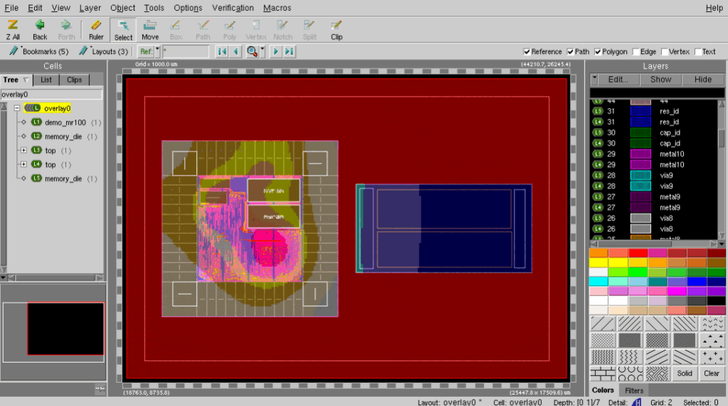
Built on proven Calibre and Flotherm technologies, Calibre 3DThermal, can perform advanced parsing of LEF/DEF, GDS and OASIS files to extract detailed die-level geometry information, enabling precise thermal property mapping and detailed semiconductor-level thermal model creation. By using Calibre 3DThermal, design teams can:
- Accurately simulate temperature gradients and hotspots
- Verify thermal impacts on electrical device behavior with die and package co-design
- Improve productivity with advanced automations such as automatic power map compression
- Enable tighter collaboration between IC and package teams
Dive deeper into 3D integration in A Guide to Heterogeneous Integration
Download this whitepaper: Conquer 3D IC thermal impacts with Calibre 3DThermal
Frequently asked questions (FAQ)
Q: What is a typical value for IC package thermal resistance?
A: It varies widely depending on the package type, die size, and cooling method. Low-power ICs may have θ<sub>JA</sub> around 100 °C/W, while high-performance flip-chip packages can be under 10 °C/W with good heatsinking.
Q: How can thermal resistance be reduced?
A: Optimize package materials, integrate heatsinks, and use simulation tools like Calibre 3DThermal to guide design decisions from early planning.
Q: Is θ<sub>JC</sub> more important than θ<sub>JA</sub>?
A: Both are important. Choose the one that matches how your heat leaves the device. θ<sub>JC</sub> is more relevant when using direct heatsinking. θ<sub>JA</sub> is used when there’s no dedicated heatsink, providing provides a broader picture, including airflow and board effects.
Q: Why simulate thermal resistance instead of measuring it?
A: Simulation with Calibre 3DThermal enables early detection of issues, reduces cost by derisking layout, materials, and cooling choices early and supports iterative optimization before tape-out. For 3D ICs, internal die temperatures and underfill effects are difficult to measure directly; simulation is the only practical lens.
Conclusion: Addressing industry’s toughest thermal challenges with Siemens
As semiconductor devices scale in power and complexity, managing IC package thermal resistance is a non-negotiable part of design success. From die-level hotspots to system-level reliability, accurate thermal modeling is essential to avoid overdesign and mitigate failure risks.
That’s why Siemens offers a comprehensive portfolio of thermal analysis tools from Calibre® 3DThermal and Innovator3D IC to Simcenter Flotherm. They scale with your design complexity and provide confidence to tackle thermal issues from early planning through sign-off.
- Accurate, efficient thermal verification
- Catch thermal issues early
- Optimize package thermal performance across 2D, 2.5D, and 3D designs
Explore Siemens’ full IC packaging ecosystem and ensure your next-generation design meets the most demanding thermal requirements with confidence.


