What about MEMS?
By Carey Robertson, Mentor Graphics
With circuit performance driven by capacitance values, accurate calculations are critical for MEMs designers.
I have written several articles in the past twelve months about the need for new parasitic extraction techniques at advanced nodes. At 20 nm, double patterning entered our lives, introducing another possible source for parasitic variation that necessitated new techniques for efficiently computing interconnect corners for parasitic modeling and electrical sign-off. That was followed by FinFET devices at 16 and 14 nm. These devices have very complex 3D geometries that require new field solver techniques to model the electrical interactions and accurately quantify the device and parasitic capacitive effects.
Today, however, we are going to jump in the WABAC machine and see what’s happening at older technologies, and the innovation there that is also driving advanced modeling techniques. The designs I want to discuss involve circuits utilizing micro-electromechanical systems (MEMs). MEMs are not unique to a particular process node, but a lot of interesting work is being done at specialized 65 and 90 nm integrated circuit (IC) process technologies.
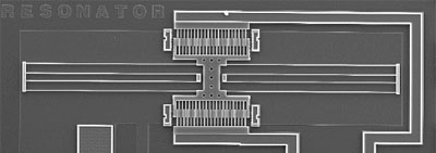
MEMs devices are designed to detect motion and deliver an electrical response. This response is monitored and leveraged across a wide range of industrial and consumer applications. You will find these devices in your automobile, smart phone and/or tablet, and video game controllers. MEMs do not utilize traditional IC components such as transistors, diodes, resistors, or inductors. Instead, MEMS consist of highly calibrated structures, as shown in Figure 1.
Figure 1. This electrostatic “comb-drive” is a common MEMS actuator, used in gyroscopes, microengines, resonators, and many other MEMS applications. (Image courtesy of Sandia National Laboratories, SUMMiT™ Technologies)
MEMs processing techniques typically leverage a combination of traditional dielectrics and airgaps to achieve a specific dielectric constant. This processing in combination with layout techniques allows MEMs designers to establish capacitive structures that are critical for the operation of the circuit. When the device is at rest, there is a “steady-state” capacitance between nodes in the devices. When the device is in motion, the capacitance will vary, which is detected by sensors in the structure.
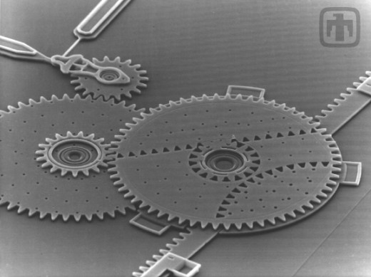
These sensors pass information to an analysis engine that can determine how fast and in which direction the device is moving. MEMs structures are incredibly complex, with high degrees of variability. Different structures are built to detect vertical motion, horizontal motion, rotational motion, etc. Figure 2 illustrates one possible configuration, but the variation in the layout and the processing is limitless.
Figure 2. This gear chain converts rotational motion (top left) to linear motion, thereby driving a linear rack (lower right). (Image courtesy of Sandia National Laboratories, SUMMiT™ Technologies)
Naturally, with circuit performance driven by capacitance values, accuracy in these calculations is highly critical for MEMs designers. While designers have several options for calculating capacitances, not all of them are suitable for use with MEMs:
- “TCAD” device modeling tools: These are typically finite element analysis field solvers that are used for all types of device characterization (MOSFETS, intentional capacitors, etc.). While these tools are highly accurate, they are not optimized for large structures, and the performance of these types of solvers is too prohibitive to be used in design environments.
- Rule-based parasitic extraction tools: These are the tools traditionally used for extracting the parasitic capacitance of IC interconnect. They derive their accuracy from a process called calibration. Calibration compiles thousands or millions of structures into a library of patterns with known golden values that the rule-based tool can leverage when extracting real designs. However, the three-dimensional variation is so great for MEMs designs that assembling a universal library is impractical. It is also worth noting that MEMs capacitance is not referred to as a parasitic or unintentional capacitance value, but rather a designed capacitance. Hence, rule-based parasitic extractors are not relevant to MEMs capacitance calculation.
- Statistical or Random-Walk Field Solvers: These solvers do have the performance to consume a MEMs device and associated sensors. They also decompose the original structure, and do not require a calibration step. However, their statistical methods incur statistical error, which means there are inherent inaccuracies that are unpredictable and difficult to quantify. These types of solvers are typically not used for MEMs structures because of this inherent statistical error.
- Fully Deterministic Field Solvers: These tools provide the same advantages as the random-walk methods without the statistical inaccuracy, providing new solutions for the calculation of MEMs capacitance values.
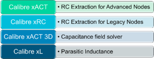
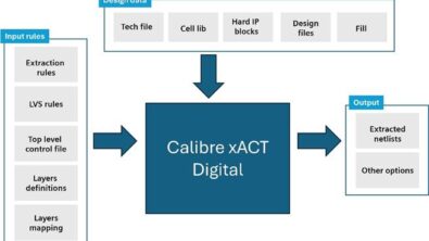
Calibre xACT 3D is an example of a fully-deterministic field solver intended for designer use. It has the performance and capacity to fully extract MEMs devices, it can model both the complex layout and the mix of dielectrics and air gaps, and it is wholly deterministic, producing accurate results without statistical error. We have worked with several companies to implement effective, accurate MEMs extraction, a process whose use should continue to grow as the industry continues to find novel applications for this technology.
Author
Carey Robertson is a Director of Product Marketing at Mentor Graphics Corp., overseeing the marketing activities for Calibre PERC, LVS and extraction products. He has been with Mentor Graphics for 15 years in various product and technical marketing roles. Prior to Mentor Graphics, Carey was a design engineer at Digital Equipment Corp., working on microprocessor design. Carey holds a BS from Stanford University and an MS from UC Berkeley. He may be contacted at carey_robertson@mentor.com.
This article was originally published on www.eetimes.com

