Stencil design considerations during library cell design

While it is widely known that library cells play a central part of the PCB design process, they also play a very important role in the design stage as well. When a new component needs to be added to a design, the first step is to evaluate physical and electrical characters of the component and consider designing a new library cell for it.
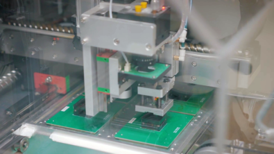
Library cell design seems to be an easy part of the entire design process, but in reality, it can be a complicated part of this process, as it involves many different aspects to consider. It should not only comply with the electrical needs, but also needs to meet manufacturing requirements. Solder paste printing is one of the manufacturing processes that may need considerations during your library cell creation. To be more straightforward, the stencil design is something need to be considered during library cell design.
Solder paste definition
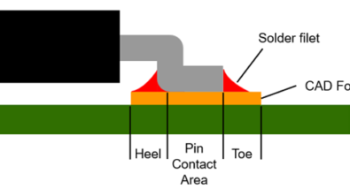
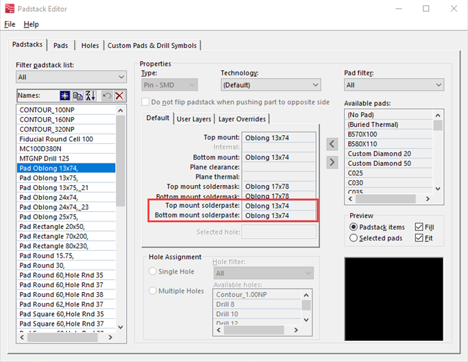
Typically, stencil design is stored as a solder paste definition in a library cell, the size of the solder paste is determined by the size of toeprint. Most times, it is using the same size of the toeprint, but that is not always the case. Some companies may also optimize the solder paste size to get a better manufacturing performance or good first yield rate.
Toeprint design
Toeprint designs need different shapes and sizes because of different package types and sizes. These need different amount of solder paste to form a proper solder joint which determines the toeprint size and solder paste definition.
A fine pitched QFN will need less solder paste deposit, so the solder paste definition or stencil aperture is relatively small, while a transformer with wide and tall termination requires a large stencil aperture to form a reliable solder joint.
IPC7351-B is a well-defined guideline that can be used to design the toeprint and determine the solder paste definition for different package types.
Toeprint spacing consideration
Spacing between toeprint or solder paste definition is another point need to pay attention. Smaller toeprint spacing tend to cause bridging issue after the solder paste printing process, and it also may impact the stencil life.
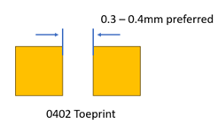
A wider toeprint spacing is good to the stencil life, but it may bring some other issues, for example, the toeprint spacing between a 0402 sized component should not exceed 0.4mm, wider spacing may cause the 0402 sized chip having higher potential to tombstone or incline during reflow process.
Toeprint size consideration
Toeprint size, as mentioned in previously, is determined by the package type. At the same time, the stencil requirement should also be considered. Typically, there is a limit to the stencil aperture size; if the aperture is too small, the solder paste is likely to adhere to the stencil wall, which results in a low printing transfer rate. This raises the question: how small can a toeprint be?
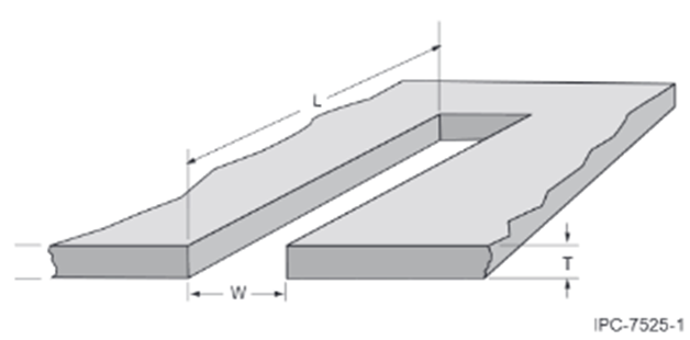
There are two golden rules to follow according to the IPC 7525 standard:
- Aspect ratio – Width of aperture (W) / Thickness of stencil foil (T) should be larger than 1.5
- Area ratio – Area of Pad (LxW) / Area of Aperture Walls (2x(L+W)/T) should be larger than 0.66
Lead position consideration
Lead position is the component lead location relative to the component body, it is also a critical factor need to consider during library design.
For example:
A wrap-rounded terminal component (Typically, a discrete component) with lead on both ends need a regular toeprint size and solder definition size defined.
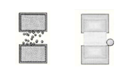
While a bottom terminal component (BTC) with lead on the bottom has a lower gap between the component body and the PCB, the solder paste volume should also be low to avoid the solder beading and component floating issue, so, a smaller toeprint size is required.
A two pin BTC is not used that frequently, but when it is placed in a design and the CAM data is sent to a stencil manufacturer, it is hard for the stencil manufacturer to know if it is a BTC component or not. Improper stencil aperture may be designed and cause the solder beading issue. Because of this, it is not bad to define the BTC toeprint properly and make a fabrication note to stencil vendor for not using a too large stencil aperture for BTC components.
Other considerations
Some other considerations are also key to a successful toeprint design:
- Missing solder paste definition As the library cell definition process is typically managed by an engineer, it is possible to miss defining the solder paste in the library cell unintentionally. Librarians should be very careful when creating the new library cell or have some intelligent tool to verify the library.
- Manufacturing process Different process requires different amount of solder paste volume. For example, the wave-soldering process and pin-in-paste process needs more solder than the reflow process and in this case, a larger toeprint is required.
- Local fiducial mark For a fine pitch component, the global fiducial mark is not sufficient to assure the accurate solder paste deposit, so a local fiducial mark may be considered in your library cell design, or alternatively, you can consider it in layout stage.
Conclusion
There are many aspects of stencil design that need to be considered in your new library cell design process, some may be critical aspects, and some may be minor aspects, but it is important to consider them earlier in your design process.
Thinking of implementing a decent DFM application to validate your library cell, is a worthy way to ensure a robust library cell creation process.