What is the PCB Design Process?
The PCB design process can be different depending on your company, but the fundamental aspects are all the same – start with a product idea and then make it into a manufacturable product. The PCB design process has both serial paths as well as parallel paths. There are also several loops for review and change. So, let’s look at the basic steps in the PCB design process.
High-level PCB specifications
The first step in the process is the creation of the high-level specifications. Here is where all the different design disciplines, marketing, electrical, and mechanical decide on the product details and schedule. Once a clear vision of the product is complete, the different disciplines are assigned their work items. Since we are focused on the PCB design process with this article, we will follow that path.
Inside the engineering disciplines there are many subgroups attached to it. Each of these groups has a specific role in the successful completion of the design. Initially, there are many parallel paths. The design engineers are identifying new components that will be needed and passing this information to the PCB librarians to create and add to the library. The signal integrity (SI) engineers will be creating their models as well as defining the stackup and constraints that will be needed. The PCB designers will be working with the mechanical engineers to define the exact dimensions of the PCB as well as identifying any critical component areas. For high volume designs this is also a very good time to start looking at assembly panelization considerations as it could affect the final board size.
Simulation and schematic entry
As that above work continues the PCB design process next steps include simulation as well as schematic entry. These two activities will be the driving force for the actual PCB design to come. There are review loops built into this process to help identify any potential issues.
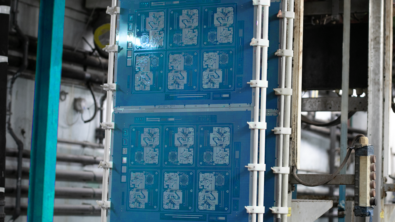
PCB layout
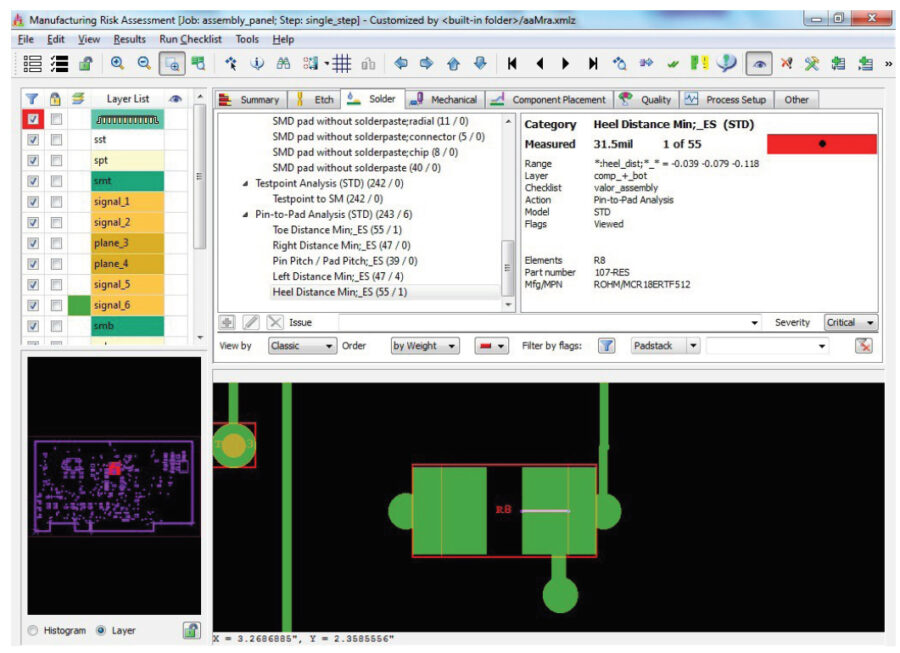
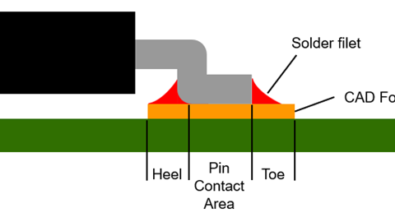
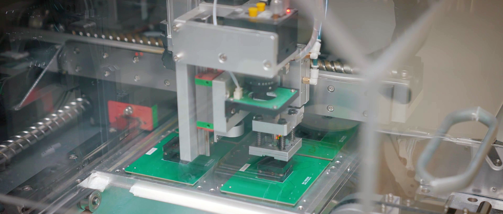
As the simulation and schematic processes wind down it’s time for the PCB Designer to start the actual layout of the PCB. This is where all the data from the SI engineers, mechanical engineers, manufacturing engineers, test engineers and electrical design engineers comes together. Now that the designer knows the outline of the PCB as well as the PCB stackup and constraint information it’s time to start placement of the components. After the initial placement is complete there is a review with the stakeholders to confirm that any mechanical restrictions as well as any manufacturing concerns are addressed. Many companies at this stage would also use Valor NPI to analyze the component placement to assure the design is manufacturable from an assembly perspective. Importing the BOM and using the Valor Parts Library can be used to check that all alternate components are compatible. Solderability analysis at this stage can catch any issues that normally are not discovered until prototyping the assembly.
Critical signal paths
The next milestone is routing any critical signals. During this step there are reviews with the electrical design engineers as well as board level simulation being run by the SI engineers. Again, Valor NPI should be used at this stage to analyze the critical routing to assure that it meets all the requirements of the fabricator(s).
Routing
Routing the remainder of the design is next. Once completed it’s on to cleaning up the design. Adjusting silkscreen and solder mask along with creating fabrication and assembly drawings is the next order of business.
DFM Review
The last major process step is to run a complete Design for Manufacturing (DFM) review. This should include both the Design for Fabrication (DFF) and Design for Assembly (DFA) analysis. All the stakeholders are present for this final review. Using Valor NPI throughout the entire PCB design process will minimize any design issues so that the PCB will be ready for the final step, once the DFM analysis has been finalized and has the approval of all stakeholders. The design can now be released to manufacturing as a clean design.
Explore Valor NPI with our Online Trial
Explore Valor NPI with our free online trial and find out how easy it is to implement the world’s most advanced DFM software. With no download or installation necessary, this simple guided tour provides immediate hands-on experience. Select your desired workflow: