Proactive Design for Test (DFT) best practices

PCB Design for Test
When you are designing a PCB, at what point do you start thinking about your test engineers? During a typical product development workflow, test points are first introduced during schematic capture. A partial list of functional test points are created and important nets are identified. Test requirements can tend to disappear then for a while, returning to the test engineer after layout for review and modification. This is an inefficient and time consuming process, but does it yield appropriately accurate results?
Test Process Preparation
If you are like many PCB designers, you begin placing test immediately following the completion of your layout. You’ve positioned components and you have a good idea of what your layout looks like, you may have even left yourself a bit of space to play with. But how do you place your test points? How do you determine what you will test? Do you place your test points where they need to go, or do you place your test points where they can go? Are your components chosen with their failure rates in mind? The answers to these questions are not always straight forward, and they reflect many of the priorities and structure of your current design and manufacturing process.
The PCB design world has been enthusiastically adopting Design for Manufacturing (DFM) practices as a quantifiable method improve production yields, but have those same designers been as enthusiastic about adopting Design for Test (DFT) best practices?
As a PCB Designer, your goal from schematic to completion is to bring the product to market as quickly and reliably and possible, while reducing overall costs. This can be accomplished by increasing yield and targeting failures to occur as early in the production process as possible. Knowing and accepting failure rate is important. PCB costs can be reduced through increasing yield by way of DFM, but costs can also be reduced by early failure identification and PCB testing. Valor NPI DFT works to help design your board specifically for testing, identifying potential functional failures during test. Decrease costly functional failures by increasing more economical test failures.
The process of DFT needs to be considered sooner and more proactively in our PCB design process. Design for testing needs to be incorporated in the schematic phase, not during the layout phase. This is when a designer should determine what nets will be needed to be tested based on their likelihood of failure and position those pins in open, accessible real-estate.
All nets are not created equally
Not all nets are created equally and not all nets fail equally. Valor NPI uses its comprehensive component understanding to provide actionable statistical analysis of your design, targeting and prioritizing nets for test based on their probability of failure. Actionable data in the design phase allowing you to design a more versatile and efficient PCB.
PCB Designing for test isn’t all about net access, its about allowing access to the proper nets. Any EDA software can assist in positioning test pins, but EDA software does not understand if a net must have a test point. When decisions must be made for which net gets test pins, you should be basing this information on numerical yields and not on accessibility after layout. Valor NPI DFT can connect the nets together and work out test point priorities, providing clear weighted decisions based on likelihood of failure.

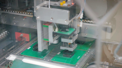
Flying Probe Testing
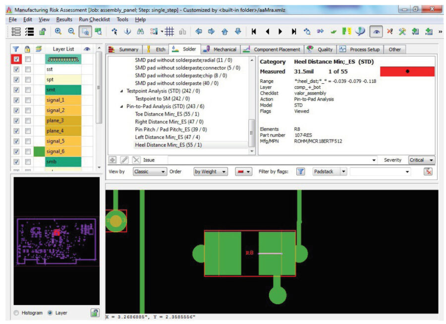
Flying Probe Testing (FPT) typically uses 4 probes suspended from a head to perform DFT. Valor NPI performs DFT Testpoint Allocation to determine adequate test point positioning. Since the contact of the FPT can be at an angle relative to the boar, the distance from each test point to other adjacent high components must be considered relative to the angle of the probe to avoid collisions.
Assuring PCB test and inspection access
An excellent resource to learn more about test point placement is the On-Demand webinar Assuring PCB test and inspection access. In this 30 minute webinar, you will learn in-depth information about how Valor NPI can be leveraged to bring your test into the design phase.
Explore Valor NPI with our Online Trial
Explore Valor NPI with our free online trial and find out how easy it is to implement the world’s most advanced DFM software. With no download or installation necessary, this simple guided tour provides immediate hands-on experience. Select your desired workflow: