Making Parts Part of Manufacturing Driven Design
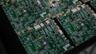
You have heard from us by now the use of the phrase “Manufacturing Driven Design,” or MDD. This is the idea that manufacturing constraints are understood fully and clearly during the design process such that potential manufacturing issues can be avoided later. Identifying, understanding and resolving issues that affect the yield, cost and reliability of a PCB is the goal of Manufacturing Driven Design and both bareboard fabrication and PCB assembly process capabilities define Manufacturing Driven Design.
Manufacturing Drive Design and PCB Assembly
When it comes to PCB assembly level MDD, many designers have not concerned themselves with the component manufacturing Bill of Material (BOM). Designers work from a CAD library that has component libraries associated with internal part numbers (IPN) their company uses. The CAD Design Rule Checking software uses those CAD library shapes for its analysis and even, in some cases, the avoidance of where components are placed. There is nothing wrong conceptually with this mentality. However, like all things, the details matter.
In today’s PCBs, the miniaturization of components, board sizes and form factor bring challenges to manufacturing that did not exist in the past. There are also pressures for lower cost and improved quality of PCBs that are impacted by the details of the electronic components used. Many companies use Automated Optical Inspection (AOI) systems inline with the SMT equipment to assure correct component placement and solder filets prior to the boards entering the reflow oven. It is imperative for the AOI system to know things like adjacent lead clearance as well as the component lead type, pitch and pin contact area. And that’s where the additional detail about parts is needed beyond what the CAD library entails. CAD libraries do not have the ability to specify the pin contact area.
From an assembly perspective, the most important concern is solderability. It has been said that when you by a drill, what you are really by is holes. Similarly, when you are paying for PCB assembly services, you are buying solder joints. You are paying for the expertise of how best to form the solder joints as well as the capability to assembly PCBs. What type and volume of solderpaste, the shape, and size of the stencil aperture all determine the quality of the solder joints.
Yet, for something that critical to the manufacturing success of a PCB, designers have not had easy tools to address solderability. In many cases, designers leave it to someone else to handle, be it a component engineer or the contract manufacturer (CM). In both of those situations, by the time an issue is identified, it is often too late to do anything about it. The boards have been fabricated and the project is behind schedule. The conversation turns to what compromises are acceptable to complete the assembly.
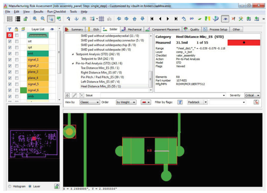
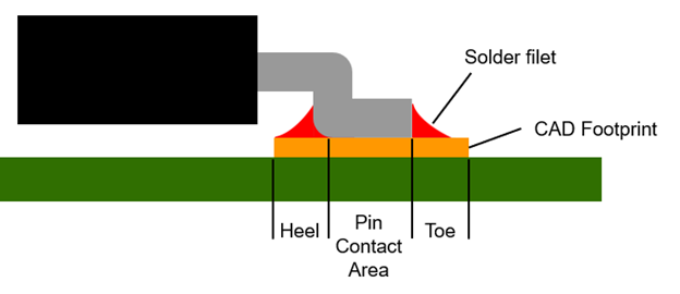
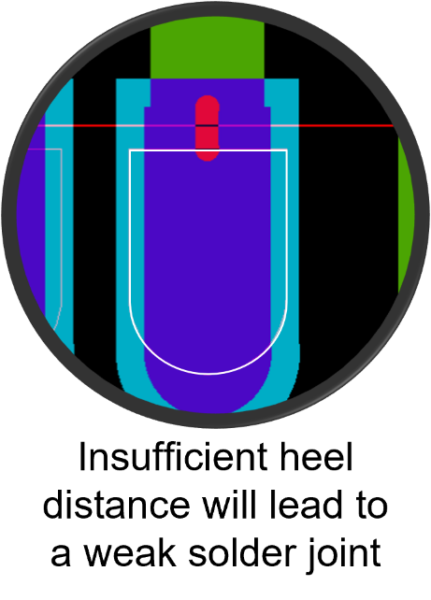
The illustration below shows that there is insufficient heel distance for a proper solder filet to form.
Performing DFM checks based on multiple footprints within your Library data increase the overall versatility of your design
The proper distance is frequently defined by IPC-7351, class 1, 2 or 3. However, in many cases a contract manufacturer will have a slightly different definition of the spacing requirement based on their experience of that lead type and solderpaste used. The same holds true for toe, side and even the ratio of heel-to-toe measurements. Similarly, there are solder filet specifications for ball grid arrays, only they are referred to as peripheral measurements. If the CAD tools do not have a mechanism for identifying and avoiding these critical process constraints, the Manufacturing Driven Design software must do so.
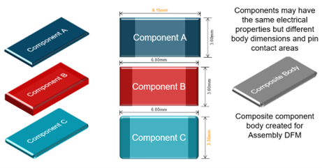
It requires the connecting of the component internal part number with the actual manufacturer’s part number. That is where the manufacturing BOM comes in. Furthermore, most companies try to qualify multiple components for a given IPN in order to provide flexibility in sourcing. The complete list of qualified alternate parts is called either the Approved Vendor List (AVL) or Approved Manufacturer List (AML). Often overlooked by many designers is the fact that components can be parametrically the same and even of the same package type, yet the actual component dimensions can vary. The question that usually doesn’t get answered until it is too late is whether those physical differences will have a negative impact on the manufacturing of the PCB.
Considering Manufacturing Process Constraints in MDD
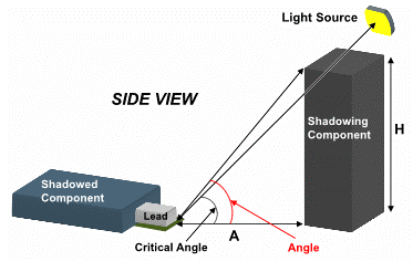
We should also consider other manufacturing process constraints that the component details can impair. For example, a tall component adjacent to another component’s leads may cause shadowing by the inline AOI camera system, making the inspection of those solder joints difficult, if not impossible.
Additionally, I have seen cases where a tall component has been placed too close to the conveyed edge of a PCB, putting it a risk of damage by the gripper on the SMT line. Usually, that happens because the designer did not know which edge was going to be used for conveyance on the SMT line, didn’t know the rule for how much clearance was needed, or did not know the exact heigh of the component.
Looking at rework, it is necessary for components that are subject to rework not to be place too close to tall components. Otherwise, the repair technician is unable to get their repair tools underneath the device being repaired. And for everyone doing electrical test in low-volume production, there are rules as to how close a tall component can be to a test point for a flying prober to have access. Not providing that clearance means those nets go untested. Another issue is component orientation. What seems clear on the CAD tool can be confusing on the assembly line. Two pin discretes as well as rectangular devices can be placed in the wrong orientation, unless the CAD pin1 location matches the BOM pin1 location.
When I discuss this topic with design organizations, they all share that they have had issues with these topics. They then start thinking about how they can improve this aspect of their design-to-manufacturing release process. In some cases, they change their design processes to provide the designers access to the manufacturing BOM and AVL. Using appropriate Manufacturing Driven Design software, they can then identify whether there will be any issues with their design in manufacturing, regardless of which components are sourced for that particular build. In other cases, the validation of alternate parts is left to the component, or sourcing engineer.
The key point here is not who does the work but rather that the design company perform this vital CAD-to-BOM/AVL validation at an early stage in the design process. Some companies are even using the MDD part library for validation of new parts in the CAD library generation process, so they know the footprints are correct for optimum solderability before the new parts are released to the CAD users for placement.
Manufacturing Driven Design encompasses all aspects of manufacturing – fabrication, assembly and test. For assembly and test, the exact component dimensions are required – body, lead type, pitch, pin contact area and pin1 indication. Performing true manufacturability analysis requires complete component details.
Explore Valor NPI with our Online Trial
Explore Valor NPI with our free online trial and find out how easy it is to implement the world’s most advanced DFM software. With no download or installation necessary, this simple guided tour provides immediate hands-on experience. Select your desired workflow: