How to Optimize PCB Design for the SMT Assembly Process Flow
PCB (Printed Circuit Board) design layout optimization is critical for the success of SMT (Surface Mount Technology) assembly. SMT assembly involves placing surface mount components directly onto the surface of the PCB, as opposed to through-hole components, which require holes to be drilled through the PCB. SMT assembly is faster, more precise, and more cost-effective than through-hole assembly, but it requires careful design optimization to ensure a successful assembly process.
The following are some tips to help you optimize your PCB design layout for SMT assembly:
1. Use Proper Footprints:
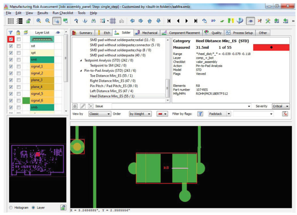
Using proper component footprints is essential to ensuring a successful SMT assembly. Component footprints define the size, shape, and location of each component on the board. The footprints should be designed according to the manufacturer’s specifications and should be accurate to ensure proper placement and alignment of each component during assembly. IPC specifications should be followed to make sure that the proper toe, heel, side, and periphery distances are maintained during soldering.
2. Component Placement:
Proper component placement is key to successful SMT assembly. Place components in a logical, easy-to-follow order. Group components that are related to each other and place them close together. This will help reduce the number of required vias and improve the electrical performance of the circuit. Placing related components close together will also help to reduce the length of the traces, which will minimize signal degradation and reduce EMI/EMC issues.

3. Keep SMT Components on One Side:
Being able to place surface-mount components on one side of the board will result in the most simplistic assembly process. This will reduce the complexity of the assembly process, increase manufacturing yield, and reduce the cost of assembly. Realistically, with the push to miniaturize products having components on both sides of the board is now the norm. This does increase the likelihood of errors during assembly as well as increase the time required to assemble the board. This practice will also reduce manufacturing yield.
4. Keep SMT Components in the Same Orientation:
All surface mount components should be placed in the same orientation (for example, with the same polarity or pin direction). This will make assembly faster and more accurate. If components are placed in different orientations, it can be difficult for the assembly machine to determine the correct orientation of each component during the inspection process. This can lead to assembly errors.
5. Avoid Overcrowding:
Avoid overcrowding components on the board as this will make the assembly process more difficult, increase the likelihood of errors, and reduce the yield. Overcrowding can also make it difficult to test and troubleshoot the board after assembly. AOI (Automatic Optical Inspection) equipment will need certain spacing requirements depending on the height of the component. Therefore, it’s important to also take the height of components into account when placing components. It is important to leave sufficient space between components to allow for proper assembly and testing.
6. Follow Design for Manufacturing (DFM) Guidelines:
DFM guidelines provide important information on how to optimize your layout for assembly and ensure that your PCB is manufactured correctly. The guidelines are typically provided by your SMT assembly house and should be followed closely. DFM guidelines include recommendations on component placement, component orientation, minimum component spacing, and other important factors that can impact the success of your SMT assembly.
7. Use Test Points:
Include test points in your design to make it easy to test and troubleshoot your board after assembly. Test points can be used to measure signals at different points on the board, which can help to identify problems or issues that arise during testing. Test points should be located in areas that are easily accessible and should be clearly marked to facilitate testing.

In addition to these tips, there are other factors that should be considered when optimizing your PCB design layout for SMT assembly. For example, it is important to consider the material and thickness of the PCB, the size and spacing of the vias, the type and size of the solder pads, and other factors that can impact the success of the assembly process.
Overall, optimizing your PCB design layout for SMT assembly
In conclusion, optimizing PCB design for SMT assembly is crucial to ensuring that the final product is functional, reliable, and cost-effective. Designing PCBs for SMT assembly requires careful planning, attention to detail, and adherence to best practices and industry standards. By following these guidelines, designers can improve production efficiency, reduce costs, and improve the performance and reliability of the final product.
Explore Valor NPI with our Online Trial
Explore Valor NPI with our free online trial and find out how easy it is to implement the world’s most advanced DFM software. With no download or installation necessary, this simple guided tour provides immediate hands-on experience. Select your desired workflow: