Optimizing PCB DFM Guidelines
Daily I receive emails containing links from PCB supplier offering quick quotes, free DFM analysis, and so on. The emails with the subject line correspond to something like a “PCB data checklist” I typically find interesting because the topic is usually related to the use of an intelligent “digital twin” leading to the production of a completed PCB. All the other topics and offerings are forms of enticement to engage in business with one supplier over another.
A Typical PCB DFM Checklist
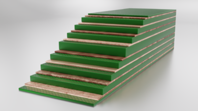
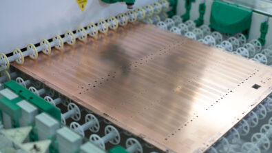
Many of these checklists to this day begin with a list of layers that need to be transferred into production as a set of files.
- One Gerber file for each copper layer.
- One Gerber file for each solder mask layer.
- One Gerber file for each silk screen layer.
- One Excellon file for each drill span layer.
- Fabrication instructions preferable in Gerber.
- In Gerber 274X format when possible.
- Netlist file in IPC-D356 or 356A.
The checklist continues to state that the fabrication instructions need to contain the following.
- One table defining the requirements for each drill span.
- Dimensioned drawing representing the board outline.
- Stackup and impedance targets.
- Other specifics such as solder mask and silk screen colors, surface finish, UL requirements, IPC requirements, panelization information, and so much more.
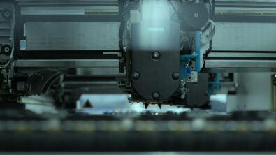
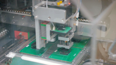
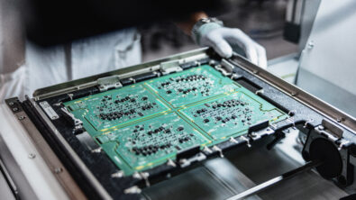
After providing this information consider what your PCB supplier is going to do and what you are asking of them. They are going to take all the files that at one point represented a completely designed PCB and reverse engineer those files back into layers defined to serve a purpose. The saving grace is if there is an IPC netlist provided then they have a chance in confirming that the have the outer layer information at least correctly positioned. Since most designs still contain simple through holes, a netlist file will only validate that the outer layers are correctly positioned. It is possible that a mistake is made placing the inner layers in the incorrect sequence. Never mind, I am sure that would never happen – until it does – and it certainly has before. This is just one possible challenge in reverse engineering a design when using legacy data formats.
Don’t rely on Legacy Formats
I put forward that relying on legacy formats, one of which was defined in 1960’s, can be described using many words other than those that define intelligent or optimize. During the 1980 and 90’s PCB CAM for fabrication what they had to offer was an optimization step and it was at that time. PCB CAM eliminated the use of physical artwork when transferring a PCB design into manufacturing and instead initially transferred the before mentioned fabrication files on magnetic tape that were then reverse engineer which led the optimization of production ready PCB artwork. That in of itself was an accomplishment. The exchange was simple and based on established formats that were already used by the OEM’s generated the PCB layer artwork series that the PCB fabricators. This process shifted right the responsibility of the artwork production to the PCB fabricator where optimization methods could be applied digitally while preparing for production, which was the intent of PCB CAM.
Since then, there has been improvements to legacy formats. Gerber 274D gave way to Gerber 274X, which today remains the leading means to digitally exchange a design into fabrication. There were a couple of industry standard led attempts to address this need. For example, IPC-350 was a single file solution with a character position requirement making it difficult to support. This also made the file very large and with one character out of position the entire design failed to transfer. Valor introduced ODB++ which already had fabrication and assembly applications support production starting back in the late 1990’s. ODB++ approached the transfer differently by placing the intelligent data in smaller files stored in organized directories where only the required content needed to be accessed. The latest direction is IPC-2581 which is another industry led standard supporting a single file approach, but this time structured using an XML schema. This again results in single large file where if the structure of the data is not just right the entire design would fail to transfer. What the use of Gerber 274X to this day has led me to conclude that no matter what format the industry effort collaborates on, it will ultimately be a solution provider that provide enough value to warrant the change. This is why Gerber 274X was so quickly accepted, followed by the elevated interested in ODB++, both of which we provided by solution provided, and is why IPC-2581 struggles to replicate the relative success of both formats.
The future of DFM formats
The next method of introducing of design into manufacturing will not be based on files. The EDA solutions could use legacy CAM, ODB++ or IPC-2581 or utilize a cloud-based interface that provides a means to place the design into data structures designed to perform this task. Some may argue that such a solution is simply replacing a format and while true, and structures will be well defined, and validation of data exchange will occur during the transfer rather than waiting later to be discovered when a user attempts to use the manufacturing files. This represents the next step in optimizing the digital transformation which began with physical PCB artwork, to legacy CAM files, to the industry’s attempt to improve upon the current thinking, and to now thinking different where the entire exchange process is truly all digital. That will be the next means of a PCB DFM checklist at it’s very best. This is just one part of my vision on where the PCB fabrication and assembly design to manufacturing needs to be prepared to be.