4 things a PCB librarian needs to know about PCB fabrication

As I discussed in a recent blog, The PCB assembly process: The 4 Things a PCB librarian must know, PCB library creation is an important and challenging part of the layout process. To be a competent PCB librarian, you need intricate and detailed knowledge across various fields. Besides component assembly knowledge, a PCB librarian also needs to understand how the PCB is going to be built by a PCB fabrication factory. The PCB fabrication process involves dozens of steps, which can often be more complicated than the PCB assembly process.
Understanding these steps and the interactions involved with them, as well as the PCB fabrication process in general is vital for your initial library creation and to ensure a seamless Design for Manufacturing (DFM) strategy for your overall design process.
The fabrication process for a PCB librarian
PCB fabrication begins when the manufacturing data set is released from the design organization and handed over to the PCB fabricator. It is the process which turns your circuit board’s virtual design into a physical board. Fabricators perform several distinct manufacturing steps to achieve this process:
- Inner Layer Imaging
- Inner Layer Etching
- Inner Layer Stackup and Lamination
- Drilling
- Outer Layer Imaging and Plating
- Outer Layer Etching
- Solder Mask
- Silk Screen
- Surface Finish
- Electrical Test
- Profiling
- Packaging and Shipping
Due to the complexity and tolerances of the manufacturing process, completing these fabrication steps undoubtedly requires a shop floor and complicated, dedicated equipment. As I am sure you can imagine, there are dozens of Design for Manufacturing (DFM) considerations which exist for the majority of these steps, and countless blog posts, articles and books have been written to summarize these. Within this blog post, I am going to focus only on those steps and DFM considerations which relate directly to the role of a PCB librarian.
As a designer of the PCB footprint, a PCB librarian needs to know several key considerations during some of these fabrication steps, namely the imaging and etching, lamination and drilling, solder mask, and silk screen steps.
Imaging and Etching
Imaging is the process of transferring PCB design circuitry from the electronic files to a film. This film is overlayed onto copper foil attached to a physical surface, typically either hard fiberglass or flexible polyimide. After this, a UV light hardens and polymerizes the clear part of the film, leaving an outline of the desired traces and pads. The polymerized film then protects the traces and pads, allowing for the remaining copper to be removed.
Etching is the process of removing the unwanted copper. Strong alkaline chemicals are used to remove the excess copper that is not protected by the polymerized film, leaving the traces and pads.
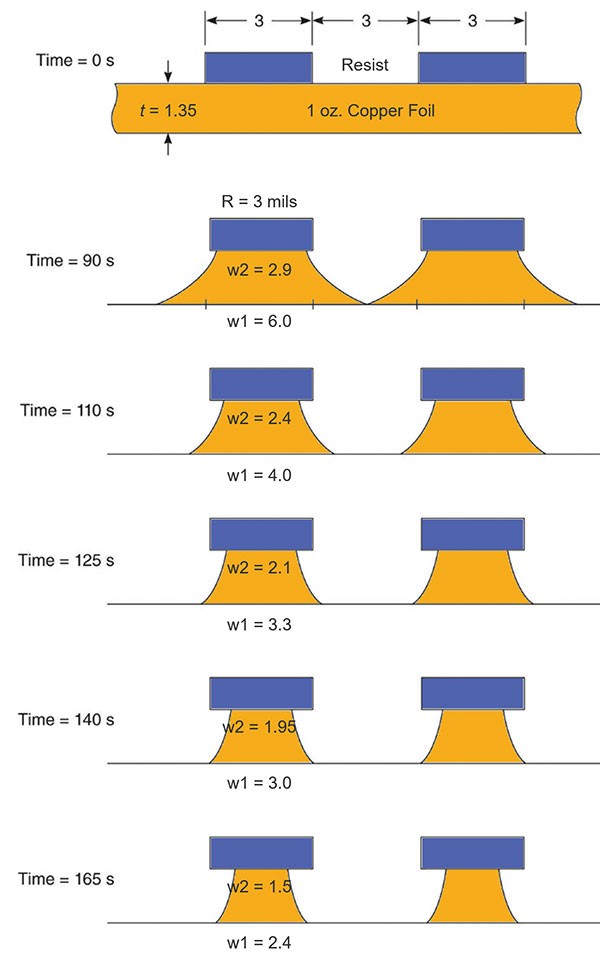
Toeprint Spacing
During the imaging process, a fabricator will alter the actual look of the design to compensate for the etching process. As the etching takes place, the process naturally removes extra copper under the film or photo resist itself, which forms what is called “undercut”, as shown in Figure 1. The toeprint spacing after compensation should meet the minimum electrical gap requirement. The thicker the copper is, the wider the toeprint spacing is required to properly etch the layer, as the thicker copper requires more etching time which results in a wider “undercut”. For this reason, a fine pitch component can not be placed on a high-power supply card with thick copper on outer layer.
Lamination and Drilling
The next step in the PCB fabrication process that a PCB librarian needs to understand is that of lamination and drilling, where the buildup for the layers is created.
Lamination is the process of using pressure and high temperature to stack and bond the individual etched layers of a PCB together, connecting and joining the multiple layers cores and prepregs together. Bonding the layers together is only half of this process.
Drilling a PCB is the second component in this general process, as additional drilling is also required to connect the layers using vias. Drilling also allows space for leaded components.
A general understanding of the manufacturing process of your board is a necessity for your overall component layout. Understanding the position of core, prepregs and laminates within the general buildup of your board, and how the interconnections and vias will be created is vital is a necessary step. The components selected do a lot to determine the overall number of layers required and the drilling sequence for the PCB as shown in Figure 2.
A single board can go through multiple lamination and drilling cycles as the complexity of the board increases.

Annular Ring
When PCB librarians are designing the annular ring for a Through Hole (TH), toeprint or via, they should consider both the copper layer alignment tolerance during lamination and drill position tolerance during drilling process. This helps to avoids the drill breakout issue. IPC 2221 has the definition of annular ring requirement for different classes of product as shown in Table 1.
| Annular Ring | Class 1, 2 and 3 |
| Internal Supported | 25.0 microns [0.000984 in] |
| External Supported | 50.0 microns [0.00197 in] |
Drill Size Tolerance
The drill size tolerance and drill figure are also important in the library creation, the tolerance is typically based on the PCB manufacturer’s capability, 2 mil is often used as the tolerance for a Plated Through Hole (PTH) or a Non-Plated Through Hole (NPTH) drill. However, a NPTH can have a smaller tolerance in size, as it does not require the plating. Without this extra process, the NPTH size can be controlled more precisely. This is another key component for a PCB librarian to keep in mind
Drill Shape & Minimum Drill Size
It may sound obvious, but drilling tools used to drill the hole always make a round shape. This needs to be reflected within the design and something a PCB librarian should always keep in mind. Designing a PCB with a rectangular or square shaped drill is unachievable by the drilling process.
Drill size is determined by the minimum drilling tool size and drilling type. Different vendors may offer different drilling capabilities and may have different sized drills available at any one time. It is not uncommon for a fabricator to drill out a larger hole with the expectation that they will plate up the difference to match the finished diameter required. This can potentially result in more copper on your PTH’s that expected. The smallest size of mechanical drill hole is typically 6 to 8 mil. Smaller holes can be created using laser drilling equipment. In this case, then the smallest drill size can be 3 to 4 mil.
A rectangular drill, or a drill in a size smaller than the fabricator’s capability needs to be avoided.
Solder Mask
Solder mask is another step that librarians need to be directly concerned with.
Solder mask is a kind of epoxy-ink printed onto both side of the outer copper. It is used to protect the copper from moisture and pollutions, and also prevents solder bridging during the assembly process.
Solder Mask Clearance
For solder mask printing position tolerance, most toeprints must be designed with a required clearance around the pad to ensure that the pad is not populated by the solder mask ink. Typically, 1.5 to 2 mil clearance is needed.
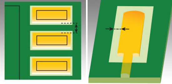
Solder Mask Web
Solder mask web is a strip of solder mask between toeprints, as shown in Figure 3. It is important for librarians to know that the solder mask web can not be designed too narrow, as it is common for it to detach from the laminate in the post-manufacturing process.
Silk Screen
In addition to the solder mask, silk screen features, like component reference designators, component outlines and some remark legends are silk-screened onto the board.
Silk Screen to Toeprint/Drill
Due to the printing tolerance, the silk screen should be placed in a certain spacing to the toeprint or drill, typically, more than 6 mil is required.
Silk Screen Refdes Width & Height
Depending on the printing capability of the screening mask or jetting machine, typically, the reference designators (Refdes) printed by a screening mask should be no smaller than 4 mil x 25 mil in line width and text height. An ink-jetting machine can print smaller Refdes, but for better identification by human eye, too small Refdes is not recommended.
Conclusion
DFM for a PCB librarian
This blog should cover most of the points that a PCB librarian needs to concern in a fabrication process. While intended directly for PCB librarians, it is also useful information that PCB designers, NPI engineers and SI engineers should also keep in mind. However, there are still a lot of other possible detailed things not being covered. Incorporating all of this fabrication knowledge into your PCB library creation process will allow you to create more robust and always-correct PCB footprints for your design. For more information on PCB manufacturing for the PCB librarian, please read my previous blog post: The PCB assembly process: The 4 Things a PCB librarian must know
Siemens provides the manufacturing driven design application which includes hundreds of PCB fabrication capabilities, that enables PCB librarians to quickly adopt all of the fabrication knowledge into the library creation process.