The PCB assembly process: The 4 Things a PCB librarian must know
Undoubtedly, PCB design is a very complex and challenging job, especially when new technologies and manufacturing processes are evolving every few years. PCB library creation is an important and challenging part of the layout process. To be a competent PCB librarian, you need intricate and detailed knowledge across various fields. PCB assembly is one of the main fields that a good PCB librarian needs to know in detail, as it is the point where your board components interact with your final design. Understanding this interaction and the PCB assembly process in general is vital for your initial library creation and to ensure a seamless Design for Manufacturing strategy early in your design process.
The PCB assembly process
When a Printed Circuit Board is fabricated by a fab shop and all materials needed for production are ready, then the PCB assembly process is launched. Sometimes assembly is performed at the same location as fabrication, but quite often it is performed at a separate location, by a second company called a PCB Contract Manufacturer (CM).
PCB assembly, sometimes referred to as PCBA, is a process to place and solder different components like resistors, capacitors, and integrated circuits onto a printed circuit board, and connect the circuit board both mechanically and electrically. Only once this is done can PCBA can achieve the expected functionality.
The assembly process varies based on the components selected in a design, however, most products involve 7 typical steps during the assembly process:
- Solder Paste Printing
- Component Placement
- Reflow Soldering
- Wave Soldering
- Screw-fastening parts assembly
- Inspection and Test
- Packaging and Shipping
These are essentially the 7 steps that a PCB needs to go through during the assembly process. While there are DFM considerations during all of these steps, we are going to focus only on those steps which relate to the role of a PCB librarian.
As a designer of the PCB footprint, a PCB librarian needs to know several key considerations during some of these assembly steps, namely the solder paste printing, component placement, reflow soldering, and wave soldering steps.
1. Solder Paste Printing
Solder paste is the soldering material used to provide mechanical and electrical connection between components and a Printed Circuit Board, the key consideration in this process is the stencil aperture that is used for applying the solder paste.
As the stencil aperture is determined based on the PCB toeprint size, most times a PCB’s toeprint size is similar in size to the stencil aperture. This makes it important to know the key points during the PCB library design stage.
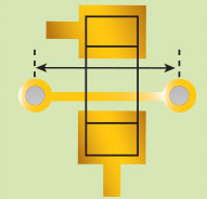
Toeprint Size
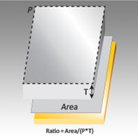
Component toeprint size should not violate the minimum size requirement of a stencil aperture. IPC-7525 is a well-defined guideline when defining the toeprint size, an aperture width ratio (width of aperture divides thickness of stencil foil) larger than 1.5 and an aperture area ratio (area of Pad divides area of aperture walls, as figure 1) larger than 0.66 is a general golden guideline for defining the toeprint size.
IPC Documentation covers hundreds of specifications designed to improve the overall reliability of a PCB throughout its product lifecycle, including many that cover the PCB Assembly process. Learn all about IPC rules in our whitepaper: How PCB designers can use IPC specifications for DFM

Different package type needs different amounts of solder paste deposit or stencil aperture, IPC-7351 provides a good guideline to define the toeprint sizes of different package types, as shown in figure 2.

Toeprint Spacing
Spacing between toeprint or solder paste definition is another point that PCB Librarians need to pay attention to. Smaller toeprint spacing tends to cause bridging issue after the solder paste printing process, and it also may impact the stencil life during PCB assembly.
Local Fiducials
A center or diagonal fiducial is required to provide precise stencil printing for a very narrow pitched toeprint.
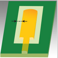
Route Keepout
For a discrete footprint, route or trace is forbidden to be placed underneath the component body or between the two toeprints, this creates an uneven surface and leads to properly address the solder paste, as shown in figure 3.
2. Component Placement
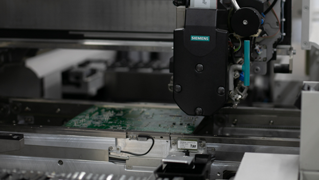
The next step of PCB assembly is component placement. A pick and place machine will assemble the components in their designated location of a PCB in an automated way. To avoid the components conflicting during the pick and place operation, the main concerns are:
Footprint Placebond
The PCB library placebond design not only needs to consider the component outline tolerances, but also needs to be concerned about the placement accuracy of the placement machine. 0.1mm of placement tolerance is a general size that contributes to a footprint placebond design, but a larger or smaller number may be used depending on the machine capabilities – a key component of the PCB assembly process.
Footprint Centroid
Footprint centroid or footprint origin is used to define the center coordinates where the component will be assembled during the pick and place process, so it is good habit to put the footprint centroid at the geometric center of a surface mount footprint.
3. Reflow Soldering
Next, boards will move through a reflow oven, which melts solder paste so that it creates a solid and reliable electrical connection between components and printed circuit boards. Reflow process also has some general requirements to the toeprint design.
Solder Mask Annular Ring
Solder mask annular ring definition is used to avoid solder mask contamination to the toeprint due to the solder mask printing tolerance. However, in the reflow process, it is also important, the solder mask annular ring can help to relief the thermal stress of BTCs(bottom terminal components) and also decrease the potential of solder bridging of a fine pitch ICs during reflow soldering. Solder mask annular ring is typically 2mil on each side, but it can be smaller if fabrication capability permits.
4. Wave Soldering
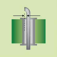
The last soldering step in the PCB assembly process is wave soldering which helps the through hole components to be soldered onto the circuit board. The through hole pins are immersed into the wave soldering machine and soldered to the printed circuit board in an automated method. Wave soldering process requires the through hole toeprint designed in an appropriate hole size and annular ring size:
TH Drill Size
IPC-2221 provides a good guideline to achieve proper wave soldering, sufficient space is required between the plated hole wall and the outer edge of the TH lead, recommended values by IPC 2221: Level A – 0.25 mm, Level B – 0.20 mm, Level C – 0.15 mm.
TH Pad Size
IPC-2221 also provides the recommended annular ring size of through hole components, Level A – 8mil + minimum fab allowance annular ring, Level B – 4.92mil + minimum fab allowance annular ring, Level C – 3.95mil + minimum fab allowance annular ring.
Conclusion
In this blog, some general requirements on the PCB assembly process are covered, but there are many more aspects that need to be considered by a PCB librarian. Incorporating all of this PCB assembly knowledge into your PCB library creation process will allow your PCB footprint to be “First time right” and “first time optimized” in the PCB assembly process.
Siemens also provides the manufacturing driven design application to help librarians to design and validate different requirements in a library creation process.

Explore Valor NPI with our Online Trial
Explore Valor NPI with our free online trial and find out how easy it is to implement the world’s most advanced DFM software. With no download or installation necessary, this simple guided tour provides immediate hands-on experience. Select your desired workflow: