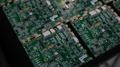
Strengthening PCB Solder Connections
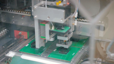
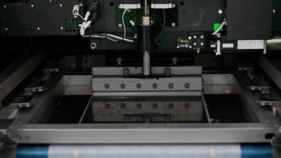
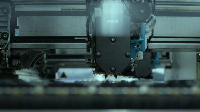
Solder is a critical part of the electronics manufacturing process, as it provides vital electrical connection to the PCB, while physically holding components in place. Solder is also the weakest part of the overall assembly, as the solder connections are both small and brittle, with the application occurring at high temperatures on very small pads, leaving little room for error. Poor quality solder joints can lead to test issues, field failures and generally lower overall yields. Correcting these issues after the fact cause unnecessary costs and delays.
To increasing the overall solder strength within a PCB design, designers should be focusing on two distinct but related factors: The material composition of the solder, and the pad and footprint layouts for individual components. The composition of the solder itself will depend upon the application of the board, the components, construction method and materials within the board, and the overall final board quality. The overall footprint of the component will be dependent upon the components within a BOM and the recommended assembly guidelines of your assemblers. Both of these factors rely on discussions and interactions with your assembly house and leaving these discussions until after the design has been released ultimately limits your assembly options.
The Strength of Solder
The reliability of solder joint connections is determined by several variables, including the physical parameters for the solder itself, this involves shear strength, creep resistance, drop shock, thermal fatigue and vibration resistance. These values depend upon the specific type of solder being used. Most solder is now Lead-free, conforming to RoHS compliance. Lead solder is typically a 60/40 mix of Tin to Lead, but removing the lead and going exclusively with Tin results is a shiny solder that is remarkably brittle.
Adding silver to a pure tin solder significantly increase the overall strength of the solder. General convention has Tin-Silver (Sn-Ag) and Tin-Silver-Copper (Sn-Ag-Cu, or SAC)[1] based solders to be the most promising alternative combinations to replace traditional Lead-based alloys. These are popular choices due to their overall wettability, as well as their consistent adherence to delicate BGA components. [2] Additional alloys can be added to the mix to change certain characteristics of the solder, but all have tradeoffs. For example, adding Bismuth to the solder lowers the melting point and increases the wettability of the solder, but it is expensive and makes the connection more susceptible to joint failure.
HMP Solder
Lead-based solders increase the melting point of the alloys being used and as the ratio of Lead to Tin increases, so does the melting point. The resultant solders can generally be thought of as High Melting Point (HMP) Solder. This temperature increase fundamentally changes the assembly process, and by necessity, the fabrication process. The result is that boards experience higher thermal cycles that aren’t necessarily required with many Tin-based solders. Increased temperatures can be particularly stressful for certain dielectric materials as the variation in temperatures can lead to flexing and delamination within the board. Because of this, a shift to resin and fiberglass dielectric materials with high Coefficient of Thermal Expansion (CTE) values has becomes increasingly important.
HMP Solder however does come with several additional benefits and is extremely useful in specific PCB applications. These solders contain between 1.5% – 5% Silver. As this ratio of silver decreases, it increases the strength and wetting power of the HMP solder. The Tin content for HMP solder can be anywhere from 5%-20%. As the ratio of Tin to Lead decreases, the solder takes on different characteristics, specifically extreme thermal conditions. At extremely low temperatures, below -70oC, low HMP solder values with Tin percentages around 5% are required to avoid operational cracking. In addition, HMP solder allows for precision soldering of adjacent joints, with the initial work being performed with HMP solder, and surrounding soldering being performed with decreasing melting points, ensuring that subsequent work does not affect the initial joint.[4]
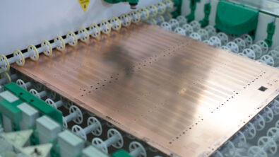
PCB Component Solder Footprint
Aside from the solder itself that is used on the joint, the other main point of consideration is the position and dimensions of the pads that make up a component’s footprint. Ensuring the overall solderability of your PCB assembly is an increasingly challenging task due to component sizes shrinking and solder paste technology evolving. Aside from this, consideration should also be taken when considering the possibility of solder rework. Designing a component footprint to meet these challenges, while also being versatile enough to allow for alternate parts can be a difficult and time-consuming process if performed manually. Automating this process so that it is performed concurrently with design, even as early as creating the library cells, assures improved manufacturability.
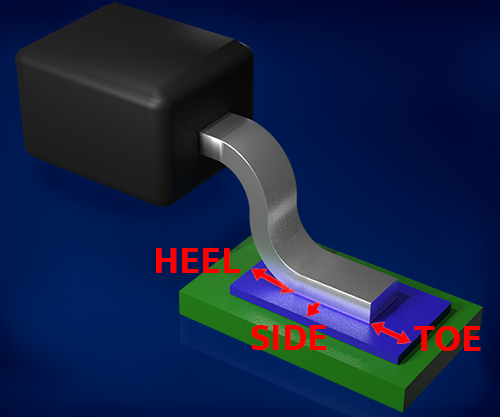
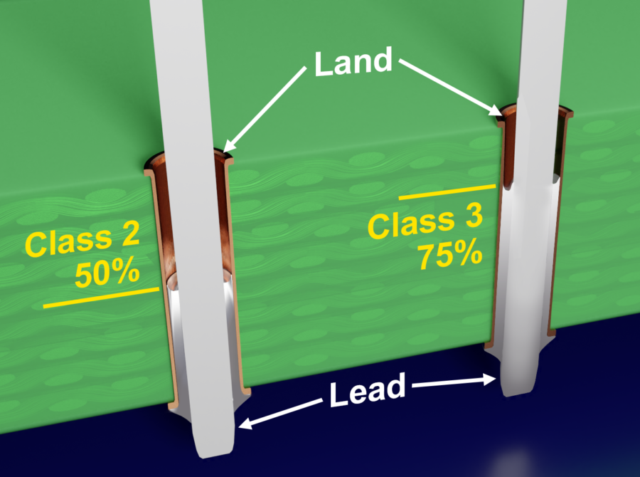
When creating new PCB library cells, pad sizes can be determined by industry component solderability standards. IPC-7351 Surface Mount Design Standards show the recommended heel, toe and side fillets for a connection. In general, deviations from these values occurs most frequently when reviewing the assembly guidelines of an assembler. They may have specific experience with a certain package type and recommend a specific unique footprint for that component.
PCB Component Parts Library
The issue that arises with controlling pad sizes and overall component footprints comes when your BOM includes alternate parts. Ensuring this pin to pad relationship continues consistently across your qualified parts can mean the creation and maintenance of countless new package information for each of these parts, coupled with versatile solder mask templates that accommodate for the shifting physical dimensions. CAD librarians often do not have visibility of all the alternate parts that may be qualified for use in manufacturing when they first create their library cells. Only later when alternate parts are identified for manufacturing does the initial footprint become an issue of fit.
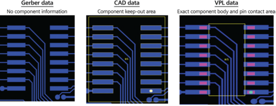
The Valor Parts library, a component of Valor NPI, consists of true pin and package information for over 250 billion manufacturing part numbers, denoting exact pin footprints for every one of your qualified parts. Being able to analyze the pin to pad relationship and spacing requirements while still in the design phase helps to assure that there will be no assembly issues when the design is manufactured.
Valor NPI and the Valor Parts Library make use of a digital twin of your design, allowing you to perform virtual validation of your solder joints using not just your primary parts, but on every possible combination of your alternate parts within your BOM. The overall assembly analysis requirements are based on the process method assigned to each component by the VPL and the components orientation to one another, such as be leaded-side or unleaded-side.
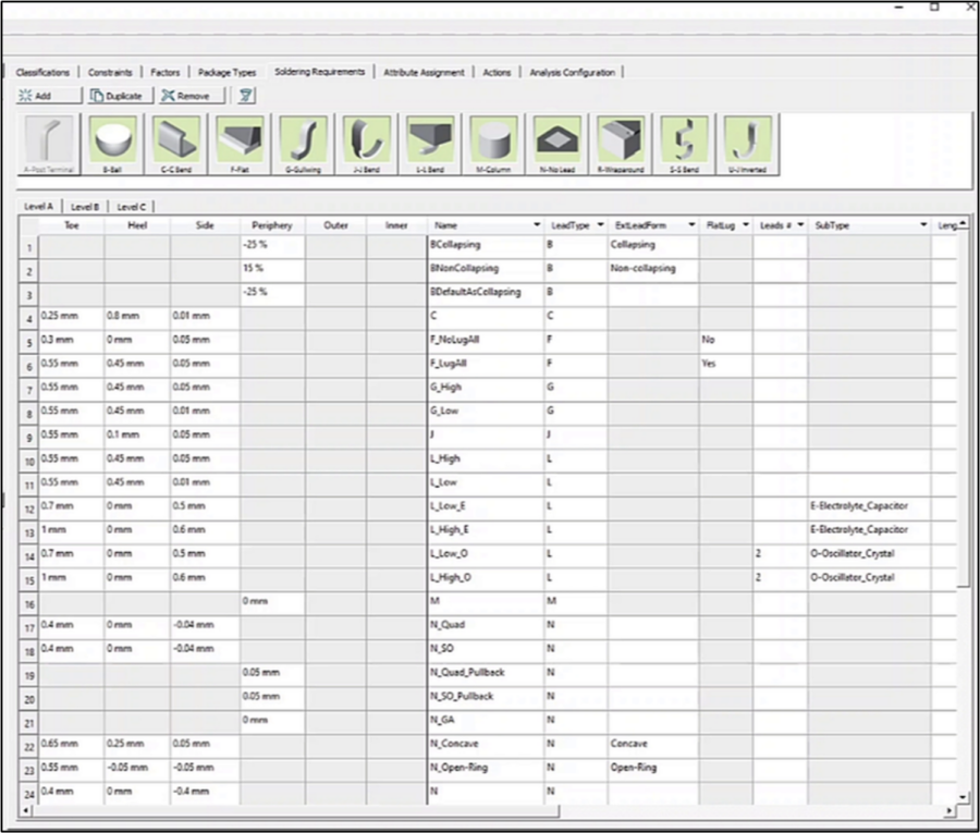
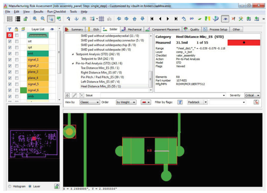
Valor NPI starts with the CAD footprint and brings in the corresponding Valor Parts Library part. Solderability checks are performed on this pin footprint, ensuring that there is a sufficient amount of heel, toe and side clearance to create a reliable connection. Once this information has been applied to a design, Valor NPI is able to identify any situations where there is a risk of solder bridging between pins, or a mismatch for fit. It identifies when an insufficient heel distance will lead to a weak solder joint. Or when an insufficient toe distance or the heel to toe ratio will affect the quality of a solder joint. Or when a side solder fillet is insignificant for the solder joint. A similar test is performed for the periphery for ball contacts.
Digital Solder Validation
Solder Validation is performed in two stages:
- Valor NPI creates a composite component body created from the dimensions of all the qualified components within the BOM or Approved Vendor List (AVL) and uses the dimensions taken from the Valor Parts Library to generate an idealized component footprint that accommodates these qualified components.
- The solderability of each these components is measured against the designated footprint.
Solder validation is where the combination of Valor NPI along with VPL really shines. Being able to analyze the pin to pad relationship while still in the design phase is vitally important. Where the pin touches the pad is absolutely the most crucial part of soldering. Ensuring that this connection and overhang is sufficient will help to improve the overall manufacturability of your PCB.
Valor NPI is delivered with the IPC-7351 and IPC-2221 solderability values in place. While those values are acceptable a high percentage of the time, you do have the ability to modify the rules based on your manufacturing partners’ requirements.
Explore Valor NPI with our Online Trial
Explore Valor NPI with our free online trial and find out how easy it is to implement the world’s most advanced DFM software. With no download or installation necessary, this simple guided tour provides immediate hands-on experience. Select your desired workflow:
[1] https://link.springer.com/article/10.1007/s10854-015-3606-y
[2] https://link.springer.com/article/10.1007/s11664-020-08525-9
[3] https://aimsolder.com/sites/default/files/the_fluidity_of_the_ni-modified_sn-cu_eutectic_lead-free_solder_white_paper.pdf