6 material properties that can save you money when designing your PCB stackup
Introduction
Stackup decisions are critical to every PCB and electronic product, but they don’t always get the attention that they deserve. With better stackup planning focusing on six key parameters, designers can select the right materials early in the design process and minimize the risk of under- and overdesigning their PCB.
Overdesigning vs. Under-designing
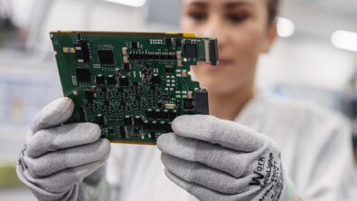
When designing your printed circuit board (PCB) stackup it is important to consider the material properties that go into your selection. All designers are aware of the pitfalls that come with under-designing a stackup—problems like signal integrity (SI) issues, manufacturing issues and general field failures can all lead to known disasters. Designers tend to overdesign their stackups to avoid these problems, but overdesign may result in unnecessary costs.
Key Parameters
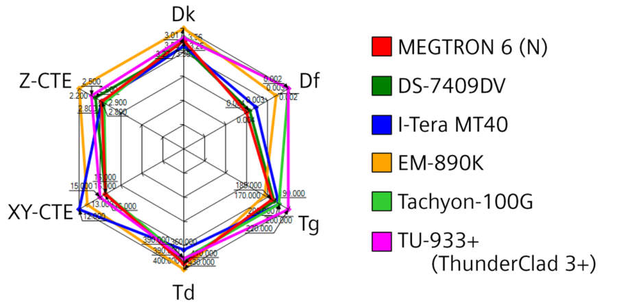
When designing any PCB stackup, there are many parameters to consider, including electrical parameters like dielectric constant (Dk) and dissipation factor or loss tangent (Df); and mechanical parameters, such as glass transition temperature (Tg), decomposition temperature (Td), and coefficient of thermal expansion (XY-CTE, Z-CTE). Other, less significant parameters include Young’s module, Poisson’s ratio, peel strength, and water absorption.
Electrical Parameters
Dk and Df values are directly related, and form a balancing act within the board as they represent the ratio between the resin and glass within the material.
Dk (Dielectric constant)
Dk is a measurement of the relative capacitance of a material in comparison to a vacuum. Low Dk values are better, as there is significantly reduced cross-talk, allowing for closer traces and thinner boards.
Df (Dissipation factor or loss tangent)
The Df value represents the energy lost through heat exchange, and again, lower is better. It is directly linked to the frequency of the board, as well as the resin content of the laminate. As the resin content ratio increases, the Df value also increases.
Mechanical Parameters
The mechanical parameters group includes thermal parameters—the physical properties of the board and how it reacts to the environment it is created in or where it will be deployed. They are important to the manufacturing process and can determine the potential deployment locations (aerospace, hot and cold climates, satellites, etc.).
Thermal parameters associated with PCB laminates are important because of the thermal excursions the PCB is exposed to during assembly and rework, and because they are affected by the thickness of an individual design. Thicker designs are more sensitive to soldering-temperature exposure because the z-directional stresses are additive and there are more places to fail.
Before the implementation of the European Union’s Restriction on the Use of Hazardous Substances (RoHs) directive went into effect in 2006, tin-lead solder, with a melting point of 185 °C, was ubiquitous in PCB assembly. Today’s lead-free solder has a melting point of 225 °C, 40 °C higher. As a result, temperatures during assembly or rework can reach >260 °C multiple times.
Tg (Glass transition temperature)
Tg is the temperature (in Celsius) at which the deformation of a laminate changes dramatically. Each material has a relatively low expansion rate until it reaches a certain temperature at which point this value will spike and start climbing quickly. By understanding the heat required to bond the board, you can understand what will be needed for transition temperatures.
Thicker boards need higher temperatures to bond uniformly. To avoid thermal expansion and delamination, the Tg value needs to reflect the nature of the board. If you have a relatively thin board, or if you can keep the number of layers down and save significantly—as much as 25% on total material costs.
Td (Decomposition temperature)
This is the temperature (in Celsius) at which a material loses 5% of its weight as a result of thermal decomposition. Since the melting point of lead-free solder is around 225°C, solder-reflow temperatures during assembly and rework will be above 225°C, and as high as 260°C. Once this point has been reached, irreversible degradation has occurred. Even loss values of 1-2% will be seen by most as unusable as the risk of delamination is simply too high.
Z-CTE and XY-CTE (Coefficient of thermal expansion)
These values represent the XY coefficient of thermal expansion and the z-axis coefficient of thermal expansion. They are different values and the practical application for this information is different, but the concept behind them is the same:
The purpose of knowing a material’s x-y-CTE is to assess the degree to which a material’s x-y expansion will differ from the x-y expansion of BGA packages, with the goal of reducing solder joint failure.
The Z-CTE reflects the thermal expansion along the thickness of the board and is linked directly to the Tg value mentioned earlier. The thicker the board, the greater the concern about stresses in the z-direction during soldering processes. Since boards are exposed to thermal excursions that exceed 225°C with lead-free solder, PCB materials with the most severe thermal expansion are going to be a significant failure concern. The thicker the board, the more you’ll want to lean toward high Tg materials and materials with comparatively low z-CTEs.
Determining when you have overdesigned
The best way to determine when you have overdesigned is to keep a robust materials library. Accurately determine your values based on detailed calculation and simulation and then bring those data points into a workable library. Being able to locate points of saving within these six material attributes allows you to explore other options and get out of your comfort zone, which is where the real savings lie. Remember that laminate prices aren’t advertised and so understanding the cost savings may require working with your laminate vendor or accepting the general rules of thumb within the document.
Summary
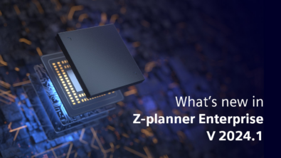
Designers are aware of the risks of under-design to signal integrity, but overdesign, which leads to unnecessary costs should also be avoided. By focusing on these six key material properties in their stackup design, designers can choose the right materials for each PCB and reduce the risk of both under- and overdesign. Learn more about materials selection in the new e-book: Stackups: The Design Within the Design. Or sign up for a free trial of Z-planner Enterprise.
Explore Valor NPI with our Online Trial
Explore Valor NPI with our free online trial and find out how easy it is to implement the world’s most advanced DFM software. With no download or installation necessary, this simple guided tour provides immediate hands-on experience. Select your desired workflow: