What materials are used in PCBS?
PCB stackup materials
These days electronic products are widely used in daily life. Starting your day with an electronic alarm clock to wake you up, then an electronic toothbrush helps you to brush your tooth, then an electronic oven bakes you some food, then an electronic car takes you to the office … it seems daily activities are inseparable from electronic products now.
As a fundamental component of electronic products, printed circuit boards (PCBs) appear in every electronic product. PCBs connect all kinds of components together, making the electronic products work in the way we expect them to. So what materials are used in PCBs? Let’s look at the PCB together.
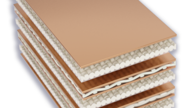
The structure of a PCB is very similar to a sandwich. Copper foil, prepregs, cores and solder mask are the basic materials that make the PCB “sandwich.”
Copper foil:
Copper foils are distributed in the top, bottom and inner PCB layers of the “sandwich”. Depending on the complexity of design, the layer count of PCB copper foil may vary from 1 to 60, and even more than that. Copper foil is a thin layer of conductive copper that is etched into circuits and patterns and then used to transfer the signals for the design.
Copper foil is classified by different thickness: 0.5oz, 1oz, 2oz, etc.
And by different manufacturing process, copper foil is classified to: ED, RA, RTF (electrodeposited/rolled annealed/reverse-treated foil)
Copper foil can also be classified by surface roughness: VLP, SVLP and HVLP (very/super/hyper low profile with average surface roughness of 7–8, 3–4 and 1.5–2 um respectively)
All different types of copper foil are used in different application scenarios.
Prepreg
Prepregs are located in the inner layers of the PCB “sandwich.” It is used as the adhesive between the copper foils. Prepreg is composed of glass fabrics and resins, the glass fabrics provide the mechanical strength, and the resins provide the viscosity.
“FR4” is a well-known and very commonly used prepreg in electronic industry for many years, but there are many other types of prepregs classified by different characteristic and performance.
Dk (Dielectric constant) and Df (Dissipation factor) are two of the commonly used characteristics to evaluate the performance of prepreg. Other characteristics include Tg (Glass transition temperature), Td(Decomposition temperature), z-axis expansion, X-y coefficient of thermal expansion.
Prepreg is classified by different glass fabric construction: 106, 1080, 2116, 3313,7628, etc., and each prepreg construction can have different resin content: ranging from 30% to 80%.
Cores
Cores can be located in the inner layers or outer layers of PCB “sandwich,” depending on the PCB stackup configuration. Cores are also known as CCL (copper clad laminates). CCL is a prepreg with copper foil cladded on both sides. As CCL contains both PP and copper foil, it has different characteristics of PP and copper foil.
Solder mask
A solder mask is an epoxy coating that covers the outer layer of copper foil for protection.
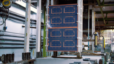
Then Cores, prepregs, copper foils and solder masks are stacked together, to form a complete PCB “sandwich” with heat and pressure.
PCB stackup is the configuration of these different materials, which provides the backbone for circuit-board design.
Many years ago, the transmission speed of PCB were very slow; most commonly used PCB materials were ED copper foil and FR4 prepreg. At that time, designing a PCB stackup was not a very complicated process, and the PCB stackup was also easy for a supplier to review. Communicating PCB stackups between PCB designers and suppliers was quite easy.
But in today’s high speed PCB design, PCB frequency becomes higher- 25Ghz and even higher frequency is nothing new – so the stackup design and corresponding PCB fabrication becomes a sophisticated job. High attention needs to be paid to the characteristics of the PCB materials – copper roughness, Dk, Df, glass-weave, resin content and so on. If the stackup is not designed well, the signal transmission in copper layers will be impacted and that may consequently cause the functional loss of the product.
How to face the challenge of the complex stackup design?
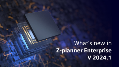
With the challenge of complex stackup design, the best practice is to use an intelligent software like Z-planner Enterprise™ to design your PCB stackup. Z-planner Enterprise™ is the only tool that enhances the stackup design process by providing a complete PCB materials library, automated stackup design wizard, as well as a design and supplier stackup comparison utility.
Z-planner Enterprise Includes:
- Everything necessary for automated design and management of PCB stackups and laminate selection, including a stackup wizard
- Interfaces to common PCB layout and signal-integrity design flows
- DFM and DFSI design-rule management and checking
- Unlimited stackup-layer support – including automated calculation of width/spacing for target impedances
- HyperLynx field solver – simulating dielectric and copper losses
- Z-solver – detailed cross-section analysis, including S-parameter export
By easily managing thousands of combinations of your PCB materials in Z-planner Enterprise™, it is the best way to get your stackup right the first time and accelerate your time to market.
Try out an online trial of Z-planner Enterprise today!