Taking 3DIC heterogeneous integration mainstream
Heterogeneous integration itself isn’t new, but new design and manufacturing technologies, combined with new product demands from system integrators, mean that heterogeneous integration and 3DIC are now becoming a necessity in mainstream design. This shift, however, is not without its challenges, as 3DIC is not a simple extension of existing packaging solutions but creates a whole new set of multiphysics integration considerations. The interaction of thermal, mechanical, reliability, test, and core semiconductor design increases complexity and requires disparate domains to seamlessly collaborate.
In this DAC 2024 webinar, Tony Mastroianni, Advanced Packaging Solutions Director, Siemens EDA, explores the challenges introduced by 3DIC, the current state of the industry to address those challenges, and the ecosystem needed to support 3DIC. Tony also discusses how users can successfully adopt 3DIC leveraging new solutions and workflows today, the importance of 3DIC design kits (3DKs) and the collaborative efforts of the Chiplet Design Exchange group to promote a chiplet ecosystem.
What are the complexities of chiplets?
A chiplet is an IC tailored for package integration. Unlike traditional IC packaging, which is straightforward with minimal IC package interaction, heterogeneous integration—placing multiple chiplets in one package—complicates the process. It requires deconstructing systems into chiplets, with considerations for thermal, signal, and power integrity demanding a comprehensive, multi-angle analysis approach.
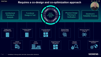
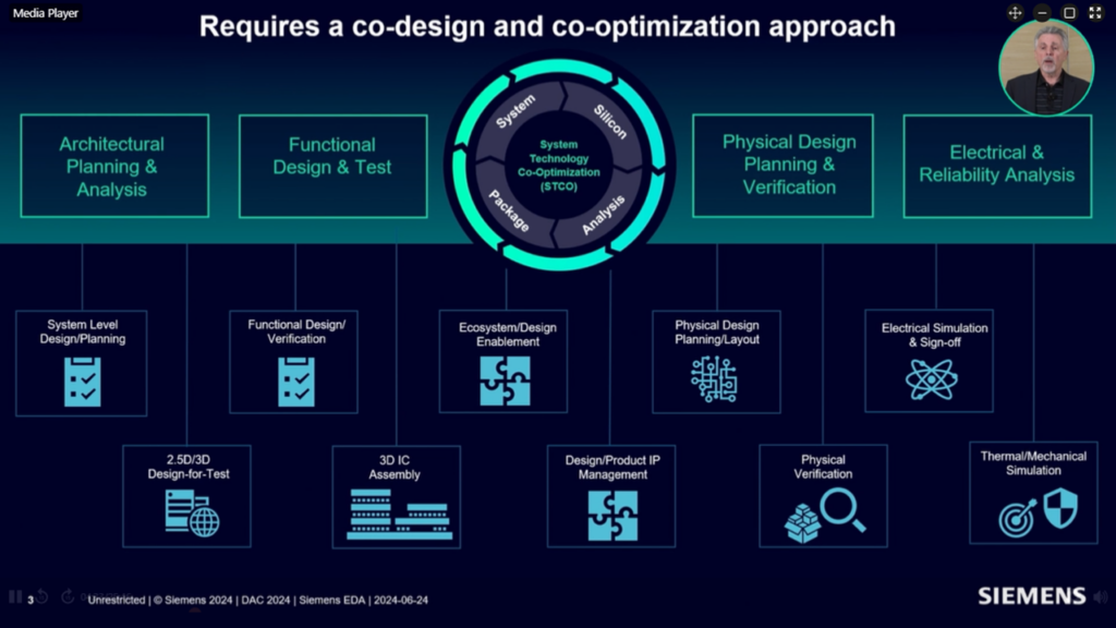
Why is system-level co-optimization important for 3DIC design?
Heterogeneous integration requires a system-level approach and technology co-optimization, incorporating everything from architectural decomposition to multi-technology implementation. It involves planning for functional simulation, verification, and testing strategies that accommodate inaccessible pins in the package. Besides choosing the right fabrication and packaging technologies (like silicon or organic interposers), designers must consider cost and non-architectural factors. Thermal management, mechanical stress, and warpage are critical due to differing thermal expansion coefficients and the proximity of chiplets.
How do digital twins help with 3DIC design?
Early predictive analysis using digital twins helps navigate 3DIC design complexities before physical design begins. Moreover, the process includes concurrent physical design and alignment of high-speed interfaces like UCIe Express and HBM among chiplets. Close collaboration is essential for ensuring signal integrity for both internal and external interfaces. The end-to-end process, from initial planning to testing the final system-in-package, encompasses physical, electrical, and reliability analyses—each crucial for delivering a successfully integrated 3DIC solution.
What is the Chiplet Design Exchange?
The Chiplet Design Exchange within OCP, is a collective that includes EDA vendors, semiconductor fabricators, outsourced semiconductor assembly and test companies (OSATs), and substrate material providers. This diverse team is dedicated to fostering a chiplet ecosystem and is involved in defining essential models and various design kits vital for the design process in this area.
What about 3DIC design kits?
There is a need for standardized design enablement resources for heterogeneous 3DIC design, which historically differs between ASIC and package design communities. ASIC design is supported by structured design kits and PDKs, whereas packaging has been less structured. The goal is to establish machine-readable formats for these design kits instead of traditional PDFs, enabling integration with design tools and workflows. Additionally, it’s crucial to have the support of the designers, EDA tools, and manufacturers like OSATs and foundries in this ecosystem.
Tom discusses how the Chiplet Design Exchange group of OCP has been actively working on standardizing chiplet design by releasing white papers that detail required design models for integrating chiplets into packages. They collaborated with JEDEC to expand the JEP30 Part Model to encompass chiplets, making it an official standard.
“With heterogeneous integration, you’re not limited to using a single ASIC technology.
Tony Mastroianni, Advanced Packaging Solutions Director, Siemens EDA
What design kits support 3DIC design?
Design enablement for IC design is highly structured, incorporating Intellectual Property (IP) blocks, Process Design Kits (PDKs) with technology and extraction rules, and pre-defined macros for memory and analog components. To support the more complex 3DIC design process, comprehensive design kits—referred to as 3DKs—are being developed, covering different aspects of the design and manufacturing process.
Currently available are Chiplet Design Kits (CDKs), with ongoing work on Package Assembly Design Kits (PADKs) to define rules for chiplet connectivity in a machine-readable, EDA-neutral format. Additionally, Material Design Kits (MDKs) aim to provide machine-readable material property data essential for analyses like thermal and stress testing. Finally, Package Test Design Kits (PTDKs) address the definition of test pin locations and modes specific to chiplet models, ensuring the necessary geometries are captured for wafer testing. This comprehensive approach to design enablement is expected to streamline the 3DIC process across various EDA tools and for manufacturers such as FABs and OSATs.
Ready to tackle the world of 3DIC? Dive into this on-demand webinar to navigate the challenges, understand industry progress, and learn about the ecosystem supporting 3DICs. Discover how you can master 3DIC adoption using Siemens EDA’s tailored solutions, including Innovator3D IC and 3DIC design kits.
To learn more about Siemens EDA 3D IC solutions, visit our 3D IC Homepage
Access our library of 3DIC resources library here.


