Enabling comprehensive DFT for chiplets and 3DICs using Tessent Multi-die
The integration and challenges of 3DIC (2.5D/3D) packaging technologies are on the rise. Among the challenges is the need for new design-for-test (DFT) strategies. DFT for chiplets must be general purpose. This is necessary so they can be tested both as stand-alone as well as easy to test after assembly into 2.5D or 3DIC devices, all the while adhering to standards like IEEE 1149.1, IEEE 1500, IEEE 1687, and IEEE 1838.
In this on-demand webinar, our expert discusses how the Tessent Multi-die solution by Siemens EDA addresses DFT for 3DIC packaging, focusing on Key IEEE standards and highlighting their relevance to testing and connectivity in complex IC architectures and emphasizing the importance of efficient testing methodologies to ensure quality and profitability in multi-die ICs, using technologies like the Streaming Scan Network (SSN) for enhanced test coverage and speed.
Introduction to 2.5D and 3DIC packaging
Advanced packaging utilizes an interposer to connect multiple dies to the package substrate, enabling heterogeneous integration. 2.5D packaging mounts dies side-by-side on an interposer, providing high bandwidth but limited integration density. 3DIC packaging stacks dies vertically using through-silicon vias (TSVs), allowing higher device density but increased complexity. A hybrid approach combines 2.5D and 3DIC schemes – some dies are mounted side-by-side on an interposer, while others are stacked with TSVs. This hybrid solution leverages the interposer to bridge the different integration methods, optimizing partitioning of functionalities while benefiting from the advantages of both 2.5D and 3DIC packaging.
Motivation for transitioning to multi-die solutions
The transition to multi-die packaging solutions is driven by the need for increased functional density to integrate more logic, data processing, and memory capabilities within a single package. By partitioning into smaller dies and combining them, higher densities can be achieved. Smaller die sizes also lead to improved yields and profitability. Additionally, multi-die packages facilitate the reuse of existing validated dies, reducing design efforts and accelerating time-to-market for new product generations. The ability to mix and match different die types enables optimized solutions tailored to specific application requirements.
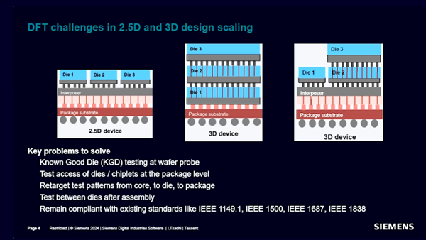
DFT challenges introduced by multi-die solutions
Multi-die packaging introduces significant DFT challenges. Early testing is required to identify non-good dies before integration, avoiding wastage. Test access becomes difficult for dies without direct package connections. Retargeting test patterns across different levels—core, die, and package—is needed to ensure comprehensive testing. New DFT methodologies must account for the limited observability and controllability of embedded dies. Overall, multi-die solutions demand innovative test strategies to enable high quality while managing rising test complexities and costs.
Overview of IEEE standards relevant to multi-die testing
Several IEEE standards address the testing challenges of multi-die packages. IEEE 1149.1 (JTAG) enables boundary scan testing, while IEEE 1687 (IJTAG) provides access to embedded instrumentation. The new IEEE 1838 standard defines test access architecture for pre-bond, mid-bond, and post-bond testing of 3D stacked ICs. These standards facilitate test pattern application and response capture for individual dies as well as the overall multi-die package. Adoption of these standards is critical for ensuring sufficient test coverage, diagnosis, and quality for complex multi-die solutions. Implementations include dedicated test controllers, on-die test circuitry, and automated test pattern translation across integration levels.
Introduction to Tessent Multi-Die Solutions
Siemens’ Tessent Multi-Die Solutions provide a comprehensive portfolio of products to address the testing challenges of advanced multi-die packages. Tessent integrates with third-party design flows and supports all major multi-die standards like IEEE 1149.1, 1687, and 1838. Released in 2024, the latest version features enhanced automation capabilities for multi-die pattern retargeting and test integration. Tessent Multi-Die Solutions allow customers to achieve high test quality and yield while managing cost through optimized test methodologies tailored for their multi-die designs.
DFT considerations for multi-die testing
Effective multi-die testing requires robust DFT techniques. Careful scan mode selection and application are needed to ensure proper test coverage across dies and the package. The use of an Enhanced Scan Network (ESN) architecture provides efficient test access and control for comprehensive testing of multi-die systems. DFT planning must account for die locations, interconnect test needs, power management, and overall quality goals. Early DFT implementation spanning pre-bond to system levels is critical for achieving a practical and cost-effective multi-die test strategy.
The flexibility and capability of using SSN as a flexible parallel port significantly enhances test time and test quality
Itamar Tsachi, Europe DFT Manager, Siemens EDA
Importance of flexible testing strategies
As multi-die complexity increases, flexible parallel testing methodologies become crucial. The SSN architecture provides a flexible parallel test port, enabling simultaneous testing of multiple dies/cores. SSN reduces overall test time through parallel operations while improving test coverage and diagnostics. Leading companies like Microsoft and Amazon have successfully implemented SSN-based strategies. In a Microsoft case study, SSN reduced their multi-die test time by 60%. Amazon leveraged SSN to enable efficient testing of their data center chips with hundreds of cores. Flexible approaches like SSN allow optimized utilization of tester resources and meet stringent test quality targets for cutting-edge multi-die products.
Detailed examination of test access architecture
In multi-die test architectures, a primary Test Access Port (TAP) provides the main test data and control interface, while secondary TAPs enable access to individual dies or stacked die groups. Configuring 3DIC test setups requires defining TAP assignments, scan paths, power domains, and test modes aligned with the device’s integration scheme. Optional features can enhance testability – for instance, flexible parallel ports like the Streaming Scan Network allow simultaneous testing of multiple dies/cores for faster test times. The primary TAP manages parallel test operations through scheduling and synchronization mechanisms. Careful planning of TAP configurations, along with intelligent use of parallel test capabilities, is key to an optimized multi-die test strategy.
Watch this on-demand webinar now to learn about Siemens’ Tessent Multi-die solution for 3DIC packaging, covering key testing standards like IEEE 1149.1, 1687, and 1838. It highlights efficient methodologies like SSN for ensuring quality and profitability in complex multi-die ICs.
To learn more about Siemens EDA 3D IC solutions, visit our 3DIC Homepage
To learn more about Tessent Silicon Lifecycle Solutions, visit the Tessent Homepage


