The multi-physics challenge: Known good die may not behave in 3D IC as stand alone!
The SoC IC model is well established. Moore’s Law continues, though without the historic economies of scale. Moving to a disaggregated chiplet approach has many advantages compared to traditional SoCs like lower costs, meeting high interconnect speeds, lower power, reduced footprint and integration of emerging technologies. Siemens 3D IC solutions address the multi-physics challenges that passing power generates and the new stresses created by 3D stacking.
Expanding from verification to multi-physics analysis
- System planning and prototyping: The system planning, and co-design cockpit integrates chiplet, die, interposer, package, and PCB to manage system-level logic definition, facilitate SIP/ASIC/Chiplet IO planning and collaboration, enable Verilog-driven chiplet design planning, define and optimize connectivity & form-factors, as well as ensure data path planning & route feasibility.
- Power/EMIR: Expanding power/EMIR integrity analysis for digital, analog, mixed-signal, and 2.5D / 3D IC supports multiple modes including a “-flow analog” based for GDSII, a LEF/DEF based flow for “-flow digital” and electro-migration and IR-drop analysis suitable for advanced node, 2.5D, and 3D IC analysis.”
- Thermal analysis: Annotating package-level thermal analysis to the chiplet/IP level performs thermal analysis at the assembly level, provides detailed information at the chiplet/IP level, offers visualization through color maps and waveforms, allows back-annotation to spice for later extraction, and is applicable in early design stages for sign-off. This ensures manufacturing issues are addressed prior to tape-out increasing yield and reducing cost.
- Stress analysis: Package level stress on chiplets includes mechanical and thermo-mechanical analysis at the assembly level, provides detailed information at the chiplet/IP level, offers visualization through stress and piezoresistive maps, allows back-annotation to spice for accurate post-assembly electrical simulation, and is applicable in early design stages for sign-off of CPI stress effects.
Meeting the multi-physics challenge
Siemens EDAs’ integrated electronic design flow encompasses planning, design, verification, analysis, post-layout simulation, and EMIR considerations. It involves physical and circuit verification techniques such as DRC, LVS, PEX, and PERC. The extended analysis flow includes Mpower models for thermal analysis, mechanical and thermal stress analysis, and feedback to EMIR. Additionally, Siemens integrates with third-party tools as appropriate.
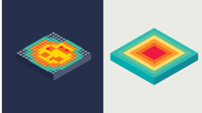
View the infographic
Explore this infographic to learn how Siemens’ EDA tackles the multi-physics challenge to achieve fast, accurate assembly-level physical verification.
FastAccurateAssemblyLevelPhysical_v2Learn more
To learn more about how Siemens 3D IC heterogeneous semiconductor packaging solutions catapult design teams into the future of IC design visit our 3D IC Homepage.
To learn about our semiconductor packaging design and verification solutions Click here.
Bookmark our semiconductor packaging blog site to keep up to date on the latest news, resources, events and more.